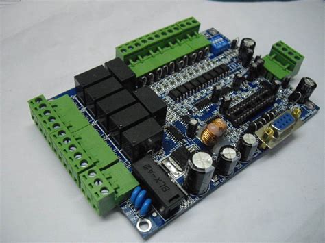
Pcb manufacturing technology
Advances In PCB Fabrication Techniques
Printed Circuit Board (PCB) manufacturing technology has undergone significant advancements in recent years, driven by the increasing demand for smaller, more efficient, and more reliable electronic devices. These advancements have not only improved the performance and functionality of PCBs but have also streamlined the manufacturing process, making it more cost-effective and environmentally friendly.
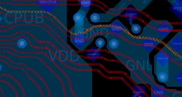
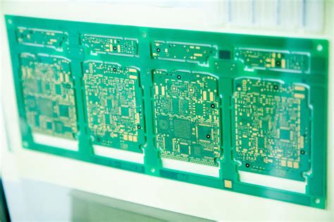
One of the most notable advancements in PCB fabrication techniques is the development of high-density interconnect (HDI) technology.
HDI PCBs are characterized by their higher wiring density per unit area compared to traditional PCBs. This is achieved through the use of microvias, finer lines and spaces, and smaller capture pads. The implementation of HDI technology allows for more complex and compact designs, which is particularly beneficial for modern electronic devices such as smartphones, tablets, and wearable technology.
In addition to HDI technology, the use of advanced materials has also played a crucial role in the evolution of PCB manufacturing.
Traditional PCBs are typically made from materials such as FR-4, a composite material composed of woven fiberglass cloth with an epoxy resin binder. However, the limitations of FR-4 in terms of thermal performance and signal integrity have led to the exploration of alternative materials. For instance, materials like polyimide and Rogers laminates offer superior thermal stability and electrical performance, making them ideal for high-frequency and high-speed applications. These advanced materials not only enhance the performance of PCBs but also contribute to their longevity and reliability.
Another significant advancement in PCB fabrication is the adoption of additive manufacturing techniques, commonly known as 3D printing.
This innovative approach allows for the creation of complex PCB structures that would be difficult or impossible to achieve with traditional subtractive methods. Additive manufacturing offers several advantages, including reduced material waste, shorter production times, and the ability to produce customized PCBs on demand. Furthermore, 3D printing enables the integration of electronic components directly into the PCB substrate, paving the way for the development of more compact and efficient electronic devices.
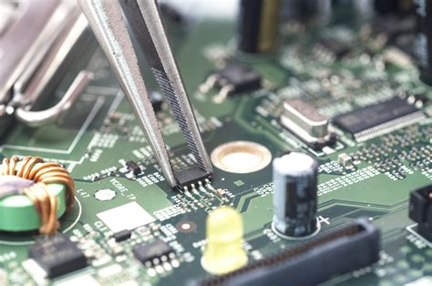
The integration of automation and artificial intelligence (AI) in PCB manufacturing has also revolutionized the industry.
Automated optical inspection (AOI) systems, for example, use advanced imaging technology and AI algorithms to detect defects and ensure the quality of PCBs during the manufacturing process. This not only improves the accuracy and efficiency of quality control but also reduces the likelihood of human error. Additionally, AI-driven design tools are being used to optimize PCB layouts, taking into account factors such as signal integrity, thermal management, and manufacturability. These tools enable designers to create more efficient and reliable PCBs while reducing the time and effort required for the design process.
Environmental considerations have also influenced advancements in PCB fabrication techniques.
The industry has seen a shift towards more sustainable practices, such as the use of lead-free solder and the implementation of more efficient waste management systems. Moreover, the development of biodegradable and recyclable PCB materials is an area of ongoing research, with the potential to significantly reduce the environmental impact of electronic waste.
In conclusion, the advancements in PCB fabrication techniques have been driven by the need for more compact, efficient, and reliable electronic devices. The adoption of HDI technology, advanced materials, additive manufacturing, automation, and AI has transformed the PCB manufacturing process, resulting in improved performance, reduced costs, and enhanced sustainability. As technology continues to evolve, it is likely that we will see further innovations in PCB fabrication, paving the way for the next generation of electronic devices.
The Role Of Automation In PCB Manufacturing
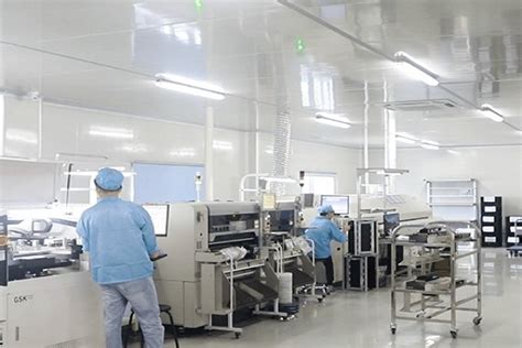
The role of automation in PCB manufacturing has become increasingly significant as the demand for high-quality, reliable, and cost-effective printed circuit boards continues to grow. Automation in this context refers to the use of advanced machinery and software to perform tasks that were traditionally done manually, thereby enhancing efficiency, precision, and consistency. The integration of automation into PCB manufacturing processes has revolutionized the industry, leading to numerous benefits that extend from the production floor to the end-user.
One of the primary advantages of automation in PCB manufacturing is the improvement in production speed.
Automated systems can operate continuously without the need for breaks, unlike human workers who require rest periods. This continuous operation significantly reduces the time required to produce each PCB, thereby increasing overall throughput. Additionally, automated machines can perform repetitive tasks with high precision, minimizing the risk of errors that can occur with manual labor. This precision is particularly crucial in PCB manufacturing, where even minor deviations can lead to significant issues in the final product.
Moreover, automation enhances the consistency and quality of PCBs.
.Automated systems are programmed to follow exact specifications, ensuring that each board produced meets the required standards. This level of consistency is challenging to achieve with manual processes, where human error can introduce variability. By reducing the likelihood of defects, automation helps manufacturers maintain high-quality standards, which is essential for applications in critical industries such as aerospace, medical devices, and telecommunications.
In addition to improving speed and quality, automation also contributes to cost savings in PCB manufacturing.
While the initial investment in automated machinery and software can be substantial, the long-term benefits often outweigh these costs. Automated systems reduce the need for manual labor, which can be a significant expense for manufacturers. Furthermore, the increased efficiency and reduced error rates associated with automation lead to lower production costs and less waste. These savings can be passed on to customers, making automated PCB manufacturing a more cost-effective solution.
Another important aspect of automation in PCB manufacturing is its role in enhancing flexibility and scalability.
Modern automated systems are highly adaptable and can be reprogrammed to accommodate different designs and production requirements. This flexibility allows manufacturers to quickly respond to changes in customer demands or market trends. Additionally, automated systems can be scaled up or down based on production needs, making it easier for manufacturers to manage varying levels of demand without compromising on efficiency or quality.
The integration of automation in PCB manufacturing also facilitates better data collection and analysis.
Automated systems are equipped with sensors and software that can monitor various parameters throughout the production process. This data can be used to identify trends, optimize processes, and predict potential issues before they become critical. By leveraging this information, manufacturers can make informed decisions that enhance overall productivity and product quality.
In conclusion, the role of automation in PCB manufacturing is multifaceted, offering numerous benefits that enhance production speed, quality, cost-effectiveness, flexibility, and data-driven decision-making. As technology continues to advance, the adoption of automation in PCB manufacturing is likely to increase, further transforming the industry and setting new standards for efficiency and reliability. The ongoing evolution of automation technologies promises to bring even greater improvements, ensuring that PCB manufacturers can meet the ever-growing demands of modern electronics with precision and excellence.
Eco-Friendly Practices In PCB Production
In recent years, the electronics industry has increasingly focused on sustainability, and printed circuit board (PCB) manufacturing is no exception. As the backbone of modern electronic devices, PCBs are integral to the functionality of countless products. However, traditional PCB manufacturing processes have been associated with significant environmental impacts, including the use of hazardous chemicals, substantial energy consumption, and the generation of electronic waste. Consequently, the industry is now adopting eco-friendly practices to mitigate these adverse effects and promote a more sustainable future.
One of the primary areas of concern in PCB manufacturing is the use of toxic chemicals, such as lead, mercury, and cadmium, which pose serious environmental and health risks.
To address this issue, manufacturers are increasingly turning to lead-free soldering techniques. Lead-free solders, typically composed of tin, silver, and copper, offer a safer alternative without compromising the performance and reliability of the PCBs. Additionally, the Restriction of Hazardous Substances (RoHS) directive, implemented by the European Union, has played a crucial role in driving the adoption of lead-free materials and reducing the presence of hazardous substances in electronic products.
Another significant aspect of eco-friendly PCB production is the reduction of energy consumption.
Traditional PCB manufacturing processes, such as etching and plating, are energy-intensive and contribute to a substantial carbon footprint. To combat this, manufacturers are investing in energy-efficient technologies and practices. For instance, the use of direct imaging technology, which employs laser beams to transfer circuit patterns onto the PCB substrate, eliminates the need for energy-consuming photomasks and reduces overall energy usage. Furthermore, implementing energy management systems and optimizing production schedules can help minimize energy waste and enhance overall efficiency.
Water usage is another critical factor in PCB manufacturing, as the process involves multiple stages of cleaning and rinsing.
Conventional methods often result in significant water consumption and the generation of contaminated wastewater. To address this, manufacturers are adopting closed-loop water recycling systems, which allow for the reuse of water within the production process. These systems not only reduce water consumption but also minimize the discharge of pollutants into the environment. Additionally, advanced filtration and treatment technologies can further purify wastewater, ensuring that any released water meets stringent environmental standards.
The management of electronic waste, or e-waste, is a growing concern as the demand for electronic devices continues to rise.
PCBs, being a fundamental component of these devices, contribute to the accumulation of e-waste. To mitigate this issue, manufacturers are exploring ways to design PCBs with recyclability in mind. This includes using materials that are easier to separate and recycle, as well as designing for disassembly, which facilitates the recovery of valuable components and materials at the end of the product’s life cycle. Moreover, initiatives such as extended producer responsibility (EPR) programs encourage manufacturers to take responsibility for the entire lifecycle of their products, including the collection and recycling of e-waste.
In conclusion, the adoption of eco-friendly practices in PCB manufacturing is essential for reducing the environmental impact of the electronics industry. By embracing lead-free materials, energy-efficient technologies, water recycling systems, and sustainable design principles, manufacturers can significantly mitigate the adverse effects associated with traditional PCB production processes. As the industry continues to innovate and prioritize sustainability, these practices will play a crucial role in promoting a greener and more responsible approach to electronics manufacturing.
Innovations In PCB Material Science
Printed Circuit Board (PCB) manufacturing technology has undergone significant advancements over the years, driven by the relentless pursuit of higher performance, miniaturization, and cost-effectiveness.
One of the most critical areas of innovation within this field is PCB material science.
The materials used in PCB fabrication play a pivotal role in determining the electrical performance, thermal management, and overall reliability of the final product. Consequently, researchers and engineers have been focusing on developing new materials and improving existing ones to meet the ever-evolving demands of modern electronics.
To begin with, traditional PCB materials such as FR-4, a composite of woven fiberglass cloth with an epoxy resin binder, have been the industry standard for many years.
However, as electronic devices become more complex and require higher frequencies, the limitations of FR-4, particularly its dielectric properties and thermal performance, have become more apparent. This has led to the exploration of alternative materials that can offer superior characteristics. For instance, high-frequency laminates, such as Rogers materials, have been developed to provide lower dielectric constants and dissipation factors, which are essential for high-speed and high-frequency applications.
In addition to high-frequency laminates, there has been a growing interest in materials that offer enhanced thermal management capabilities.
As electronic devices become more powerful, the heat generated by components can significantly impact their performance and longevity. To address this issue, materials such as metal-core PCBs (MCPCBs) have been introduced. MCPCBs incorporate a metal core, typically aluminum or copper, which helps to dissipate heat more effectively than traditional FR-4 substrates. This innovation is particularly beneficial for applications such as LED lighting, power supplies, and automotive electronics, where efficient thermal management is crucial.
Moreover, the push for miniaturization and increased functionality in electronic devices has led to the development of advanced materials that enable the production of thinner and more flexible PCBs.
Flexible PCBs, made from materials like polyimide, offer several advantages over rigid PCBs, including reduced weight, improved durability, and the ability to fit into compact and irregularly shaped spaces. These properties make flexible PCBs ideal for applications in wearable technology, medical devices, and aerospace, where space and weight constraints are critical considerations.
Another noteworthy innovation in PCB material science is the advent of environmentally friendly materials.
As the electronics industry faces increasing pressure to adopt sustainable practices, researchers have been working on developing materials that are not only high-performing but also environmentally benign. For example, halogen-free laminates have been introduced to reduce the environmental impact of PCBs. These materials eliminate the use of halogenated flame retardants, which can release toxic substances when burned, thereby contributing to a more sustainable manufacturing process.
Furthermore, advancements in nanotechnology have opened up new possibilities for PCB materials.
The incorporation of nanomaterials, such as graphene and carbon nanotubes, into PCB substrates has shown promise in enhancing electrical conductivity, thermal management, and mechanical strength. These nanomaterials can potentially revolutionize PCB manufacturing by enabling the production of ultra-high-performance boards that can meet the demands of next-generation electronic devices.
In conclusion, innovations in PCB material science are playing a crucial role in shaping the future of electronic devices. By developing new materials and improving existing ones, researchers and engineers are addressing the challenges posed by higher performance requirements, thermal management, miniaturization, and sustainability. As the electronics industry continues to evolve, the ongoing advancements in PCB material science will undoubtedly contribute to the creation of more efficient, reliable, and environmentally friendly electronic products.