PCB Mass Production: Processes, Challenges, and Best Practices
Introduction to PCB Mass Production
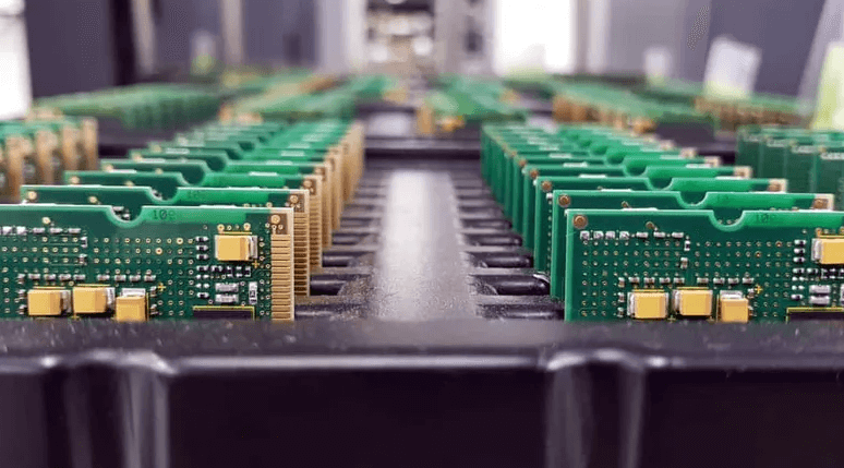
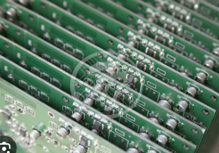
Printed Circuit Board (PCB) mass production is a complex, multi-stage manufacturing process that transforms raw materials into functional electronic components used in virtually all modern electronic devices. As the backbone of electronics manufacturing, PCB production has evolved significantly since its inception in the early 20th century to meet the growing demands for smaller, faster, and more reliable electronic products.
The global PCB market was valued at approximately $70 billion in 2022 and continues to grow at a steady pace, driven by increasing demand from consumer electronics, automotive, aerospace, and industrial applications. Mass production techniques enable manufacturers to produce thousands or even millions of PCBs with consistent quality while maintaining cost efficiency.
This article provides a comprehensive overview of PCB mass production, covering the entire manufacturing workflow, key technologies, quality control measures, common challenges, and emerging trends in the industry.
PCB Mass Production Process Flow
1. Design and Pre-production Preparation
The mass production process begins long before physical manufacturing starts. Careful preparation is essential for successful large-scale PCB manufacturing:
- Design Verification: Engineers thoroughly check the PCB design files (typically in Gerber format) for any errors or manufacturability issues. This includes verifying trace widths, spacing, hole sizes, and layer alignment.
- Design for Manufacturing (DFM) Analysis: Specialized software analyzes the design to identify potential production problems and suggests optimizations for better yield.
- Panelization: Individual PCB designs are arranged in panels (typically 18″ × 24″) to maximize material usage and production efficiency. Panel designs include breakaway tabs or scoring lines for later separation.
- Tooling Preparation: Manufacturers create stencils, drilling programs, and other necessary tooling based on the design specifications.
2. Material Selection and Preparation
The choice of materials significantly impacts the PCB’s performance, durability, and cost:
- Substrate Materials: FR-4 (flame-retardant fiberglass epoxy) is most common, but high-frequency applications may use Rogers or Teflon materials. For flexible circuits, polyimide is typically used.
- Copper Foil: Available in various weights (commonly 0.5 oz to 2 oz per square foot), with different surface treatments for improved adhesion.
- Prepreg: Partially cured dielectric material used to bond layers in multilayer boards.
3. Imaging and Pattern Transfer
The circuit pattern is transferred to the copper-clad laminate:
- Cleaning: The copper surface is cleaned and micro-etched to ensure proper adhesion of the photoresist.
- Photoresist Application: A light-sensitive chemical (either liquid or dry film) is applied to the copper surface.
- Exposure: UV light passes through a photomask (containing the circuit pattern), hardening the exposed photoresist.
- Development: The unexposed photoresist is washed away, leaving the desired circuit pattern protected.
4. Etching
The unprotected copper is chemically removed:
- Acidic Etching: Typically using ammonium persulfate or ferric chloride solutions.
- Alkaline Etching: More common for fine-line circuits, using ammonia-based solutions.
- Etch Compensation: Account for the undercutting effect by adjusting the original artwork.
5. Multilayer Lamination
For multilayer PCBs (4+ layers), the individual layers are aligned and bonded:
- Layer Stackup: Inner layers are arranged with prepreg sheets between them.
- Lamination: Heat and pressure are applied to cure the prepreg and bond the layers.
- Optical Alignment: Registration holes or targets ensure precise layer-to-layer alignment.
6. Drilling
Holes for through-hole components and vias are drilled:
- Mechanical Drilling: High-speed CNC machines drill holes as small as 0.1mm diameter.
- Laser Drilling: Used for microvias in HDI (High Density Interconnect) boards.
- Deburring: Removes rough edges left by the drilling process.
7. Plating and Surface Finishing
- Electroless Copper Deposition: Creates a thin conductive layer in holes.
- Electroplating: Builds up copper thickness in holes and on surfaces.
- Surface Finishes: Options include HASL (Hot Air Solder Leveling), ENIG (Electroless Nickel Immersion Gold), OSP (Organic Solderability Preservative), and immersion silver.
8. Solder Mask Application
A protective polymer layer is applied:
- LPI (Liquid Photoimageable) Solder Mask: Most common method, similar to photoresist process.
- Curing: UV exposure followed by thermal curing.
9. Silkscreen Printing
Component identifiers and other markings are added:
- Legend Printing: Typically white epoxy ink, though other colors are available.
- Curing: Thermal or UV curing based on ink type.
10. Electrical Testing
- Flying Probe Test: Movable probes check connectivity on random samples.
- Fixture-Based Testing: Dedicated test fixtures for 100% testing in mass production.
- Automated Optical Inspection (AOI): Cameras verify proper assembly and soldering.
11. Panel Separation and Final Inspection
- Routing/V-Scoring: Separates individual PCBs from the panel.
- Final QC: Visual inspection and functional testing of random samples.
Key Technologies in Modern PCB Mass Production
1. High-Density Interconnect (HDI) Technology
HDI PCBs feature finer lines, smaller vias, and higher connection pad density:
- Laser-drilled microvias (≤0.1mm diameter)
- Sequential lamination processes
- Any-layer via structures in advanced designs
2. Automated Optical Inspection (AOI)
Advanced vision systems perform:
- Pre-lamination inspection of inner layers
- Post-etching pattern verification
- Solder mask and silkscreen quality checks
3. Advanced Plating Techniques
- Pulse plating for more uniform copper deposition
- Direct metallization processes eliminating chemical copper
- Selective plating for high-reliability applications
4. Industry 4.0 Integration
- IoT-enabled equipment monitoring
- AI-driven process optimization
- Digital twin simulations for process improvement
Quality Control in PCB Mass Production
Maintaining consistent quality across large production runs requires rigorous quality control measures:
1. In-process Quality Checks
- Material Inspection: Verifying material certifications and properties
- Process Parameter Monitoring: Tracking temperature, pressure, chemical concentrations
- Dimensional Verification: Measuring critical features at each stage
2. Testing Protocols
- Electrical Testing: Continuity, insulation resistance, impedance
- Environmental Testing: Thermal cycling, humidity exposure
- Mechanical Testing: Peel strength, solderability, hole wall quality
3. Certification Standards
- IPC-A-600: Acceptability of Printed Boards
- IPC-6012: Qualification and Performance Specification for Rigid PCBs
- ISO 9001: Quality Management Systems
- UL Certification: Safety standards compliance
Challenges in PCB Mass Production
1. Yield Optimization
Even small defects can significantly impact overall yield in high-volume production:
- Typical yields range from 90-98% for standard boards
- Complex designs may have yields below 85%
- Six Sigma methodologies help reduce variation
2. Material Consistency
- Laminate quality variations
- Copper foil roughness differences
- Prepreg resin content fluctuations
3. Process Control
- Etching uniformity across large panels
- Registration accuracy in multilayer boards
- Plating thickness consistency
4. Environmental Regulations
- Wastewater treatment for etching chemicals
- Air emissions control
- Hazardous material handling (lead, formaldehyde)
Best Practices for Successful PCB Mass Production
1. Design Optimization
- Follow manufacturer’s design rules
- Include adequate testability features
- Design for panelization efficiency
2. Supplier Qualification
- Audit potential manufacturers
- Review their process control systems
- Evaluate their technical support capabilities
3. Prototype Validation
- Build and test prototypes before mass production
- Verify manufacturability
- Identify potential yield issues early
4. Continuous Improvement
- Analyze defect patterns
- Implement corrective actions
- Monitor process capability indices
Future Trends in PCB Mass Production
1. Additive Manufacturing
- Semi-additive processes for fine features
- Fully additive processes under development
- Potential for reduced material waste
2. Embedded Components
- Passive components within the PCB layers
- Active component embedding technologies
- Improved signal integrity and miniaturization
3. Sustainable Manufacturing
- Lead-free and halogen-free materials
- Water-based processes replacing solvents
- Improved recycling and waste reduction
4. Advanced Materials
- High-frequency laminates for 5G applications
- Thermally conductive substrates for power electronics
- Stretchable circuits for wearable devices
Conclusion
PCB mass production is a sophisticated manufacturing process that balances precision, speed, and cost-effectiveness to deliver the essential components powering modern electronics. As technology advances, PCB manufacturers continue to innovate in materials, processes, and quality control methods to meet the ever-increasing demands for higher performance, greater reliability, and more compact designs.
Successful mass production requires close collaboration between designers and manufacturers, rigorous process control, and continuous improvement efforts. With the rapid growth of IoT, 5G, automotive electronics, and other emerging technologies, PCB mass production will remain a critical industry supporting global technological progress.
Understanding the complexities of PCB manufacturing helps electronics companies make better design decisions, select appropriate manufacturing partners, and ultimately bring higher quality products to market faster. As we look to the future, innovations in additive processes, embedded components, and sustainable manufacturing promise to further transform PCB mass production in the years ahead.


