PCB Milling: A Comprehensive Guide to Precision Circuit Board Fabrication
Introduction to PCB Milling
Printed Circuit Board (PCB) milling is a subtractive manufacturing process that uses computer-controlled milling machines to remove copper from a substrate to create electrical pathways and isolation areas. This method of PCB fabrication has gained significant popularity among engineers, hobbyists, and small-scale manufacturers due to its precision, flexibility, and ability to produce prototypes quickly without the need for chemical etching.
Unlike traditional PCB fabrication methods that rely on photolithography and chemical etching, PCB milling is a clean, dry process that generates minimal waste. The technique is particularly valuable for rapid prototyping, allowing designers to iterate their circuits quickly and test modifications in real-time. With advancements in CNC (Computer Numerical Control) technology, PCB milling has become more accessible and affordable, enabling even small workshops and educational institutions to produce high-quality circuit boards on demand.
The PCB Milling Process
1. Design Preparation
The PCB milling process begins with the creation of a digital design using Electronic Design Automation (EDA) software. Popular programs like KiCad, Eagle, or Altium Designer allow engineers to layout their circuit schematics and convert them into board designs. These software packages generate Gerber files—the industry standard for PCB fabrication—which contain all the necessary information about copper layers, drill holes, and board outlines.
For PCB milling specifically, the design must be converted into toolpaths that the milling machine can follow. This conversion is typically done using specialized CAM (Computer-Aided Manufacturing) software that translates the Gerber files into G-code, the programming language that controls CNC machines. The CAM software allows operators to define critical parameters such as milling depth, tool selection, and cutting speeds.
2. Material Selection and Preparation
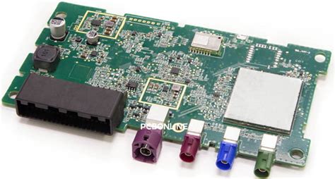
PCB milling can be performed on various substrate materials, with the most common being FR-4, a glass-reinforced epoxy laminate. The substrate comes pre-coated with a thin layer of copper, typically ranging from 0.5 oz to 2 oz per square foot (17 μm to 70 μm thick). The choice of copper thickness depends on the current requirements of the circuit and the precision needed for fine-pitch components.
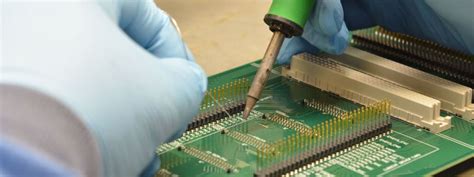
Before milling, the copper-clad board must be securely fastened to the milling machine’s work surface. Proper securing is crucial to prevent any movement during the milling process, which could lead to inaccuracies or tool breakage. Many milling machines use vacuum tables or specialized clamps to hold the substrate firmly in place.
3. Tool Selection and Setup
The selection of appropriate milling tools (bits) is critical for achieving high-quality results. PCB milling typically uses three types of bits:
- End mills: For removing larger areas of copper and creating board outlines
- V-bits (engraving bits): For creating fine traces and isolation paths
- Drill bits: For creating through-holes and vias
The most commonly used V-bit angles are 30° and 60°, with the choice depending on the required trace width and precision. Smaller angle bits can create finer traces but may be more fragile and require slower feed rates.
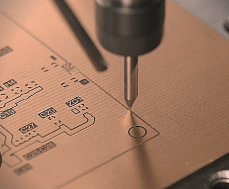
Tool setup involves carefully measuring and setting the Z-axis zero point—the point where the tool just touches the copper surface. Modern PCB milling machines often include automatic tool measurement systems to ensure precise depth control.
4. Milling Operations
The actual milling process typically follows this sequence:
- Surface leveling (optional): If the copper-clad board isn’t perfectly flat, a surface leveling operation can be performed to create a uniform working surface.
- Isolation milling: The machine removes copper to create isolation channels between traces, following the designed circuit pattern.
- Drilling: Holes for through-hole components and vias are drilled using appropriately sized bits.
- Contour cutting: The board outline is cut, separating the PCB from the surrounding material.
- Edge finishing (optional): Additional milling operations can create beveled edges or slots if required.
Throughout the process, proper chip evacuation is essential to prevent recutting of removed material, which can affect surface quality. Some machines incorporate vacuum systems or compressed air to clear chips from the work area.
Advantages of PCB Milling
Rapid Prototyping Capabilities
PCB milling offers unparalleled speed in prototyping. While traditional PCB fabrication methods might take days or weeks when outsourcing, milling allows for same-day turnaround. Designers can go from concept to physical board in hours, enabling rapid iteration and testing. This speed is particularly valuable in research and development environments where time-to-market is critical.
Design Flexibility and Iteration
The digital nature of PCB milling means design changes can be implemented quickly without the need for new masks or screens as required in chemical etching. This flexibility allows engineers to test multiple versions of a design efficiently and make on-the-fly adjustments to trace widths, component placements, or board geometries.
No Chemical Processing
Unlike etching processes that require hazardous chemicals like ferric chloride or ammonium persulfate, PCB milling is a clean, dry process. This eliminates concerns about chemical disposal, storage, and handling, making it more environmentally friendly and safer for educational or home workshop environments.
Precision and Control
Modern CNC milling machines can achieve remarkable precision, with high-end systems capable of creating traces as narrow as 0.1 mm (4 mil) or smaller. This level of control allows for the fabrication of complex, high-density designs that would be challenging with traditional etching methods.
Multi-layer Capabilities (with Limitations)
While primarily used for single and double-sided boards, some advanced PCB milling systems can produce multi-layer boards through careful alignment and bonding processes. However, this remains more challenging than with conventional PCB fabrication methods.
Limitations and Challenges
Material Waste
As a subtractive process, PCB milling generates waste material in the form of copper dust and substrate particles. While this is less hazardous than chemical waste from etching, it still represents inefficiency in material usage compared to additive processes like inkjet printing or 3D printing of circuits.
Tool Wear and Maintenance
The small diameter tools used in PCB milling are subject to wear, especially when working with abrasive materials like FR-4. Frequent tool changes may be necessary for consistent quality, adding to operational costs. Proper maintenance of the milling machine, including regular lubrication and calibration, is essential for maintaining precision.
Limited Production Scale
While excellent for prototyping and small batch production, PCB milling doesn’t scale economically for mass production. The serial nature of the milling process makes it significantly slower than photolithographic methods when producing large quantities of identical boards.
Surface Finish Considerations
Milled PCBs typically have a different surface finish than chemically etched or professionally manufactured boards. The milling process leaves microscopic tool marks that may affect solderability or high-frequency performance. Additional finishing steps like tinning or surface coating may be required for certain applications.

Best Practices for Quality PCB Milling
Optimal Feed Rates and Speeds
Finding the right balance between spindle speed (RPM) and feed rate (mm/s or in/min) is crucial for clean cuts and tool longevity. Generally:
- Higher spindle speeds with moderate feed rates work well for fine traces
- Lower speeds with higher feed rates are better for material removal and outline cutting
Manufacturers typically provide recommended settings for their tools and materials.
Proper Depth Control
Setting the correct milling depth is critical:
- For isolation milling, the depth should be slightly more than the copper layer thickness to ensure complete isolation
- For board cutting, the depth should completely penetrate the substrate without excessively cutting into the machine bed
Automatic depth sensing can significantly improve consistency.
Regular Machine Maintenance
- Keep linear rails and lead screws clean and lubricated
- Regularly check and adjust machine alignment
- Replace worn collets to prevent tool runout
- Clean the work area to prevent debris buildup
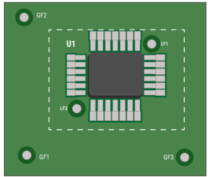
Design Considerations for Milled PCBs
- Allow slightly wider traces than minimum achievable width for reliability
- Include larger pads for vias and through-hole components
- Consider adding test points for prototyping
- Use rounded corners in board outlines for smoother milling
Applications of PCB Milled Boards
Prototyping and Development
PCB milling is ideal for engineering prototypes where rapid iteration is needed. Designers can test circuit concepts, measure performance, and make modifications quickly without waiting for external fabrication.
Education and Training
Many universities and technical schools use PCB milling machines to teach electronics design and manufacturing principles. The immediate feedback and hands-on nature of the process make it an excellent educational tool.
Custom and Low-volume Production
For specialized equipment, scientific instruments, or niche products where production volumes are low, PCB milling offers a cost-effective manufacturing solution without minimum order quantities.
RF and High-frequency Circuits
The precision of PCB milling allows for controlled impedance traces and careful geometry management important in RF applications. Designers can quickly experiment with different trace geometries and matching networks.
Repair and Modification
Milling machines can be used to modify existing PCBs or repair damaged traces, offering valuable rework capabilities not available with other fabrication methods.
Future Trends in PCB Milling Technology
Improved Automation
Future PCB milling systems will likely incorporate more automated features such as:
- Automatic tool changers for different operations
- Machine vision for alignment verification
- Real-time adaptive control adjusting parameters based on tool wear
Hybrid Manufacturing
Combining PCB milling with other technologies like:
- Additive deposition for creating conductive traces
- Laser processing for ultra-fine features
- 3D printing for creating three-dimensional circuit structures
Enhanced Precision
Advancements in motion control and vibration damping will enable even finer features and higher accuracy, potentially reaching the precision levels currently only available with photolithography.
Smart Software Integration
Tighter integration between design software and milling machines will streamline the workflow, reducing setup time and potential for errors. AI-assisted toolpath optimization could improve milling efficiency and quality.
Conclusion
PCB milling represents a powerful tool in the electronics designer’s arsenal, offering unique advantages in speed, flexibility, and accessibility. While it may not replace traditional mass production methods for high-volume applications, its value in prototyping, education, and specialized manufacturing is undeniable. As the technology continues to evolve with improvements in precision, automation, and integration with other manufacturing processes, PCB milling will likely play an increasingly important role in the electronics development ecosystem.
For engineers and makers, understanding PCB milling capabilities and limitations enables informed decisions about when to use this fabrication method versus alternatives. By following best practices in design, machine operation, and maintenance, users can consistently produce high-quality circuit boards that meet their project requirements. As the barrier to entry continues to lower with more affordable and user-friendly machines, PCB milling promises to democratize circuit board fabrication further, empowering more innovators to bring their electronic ideas to life.