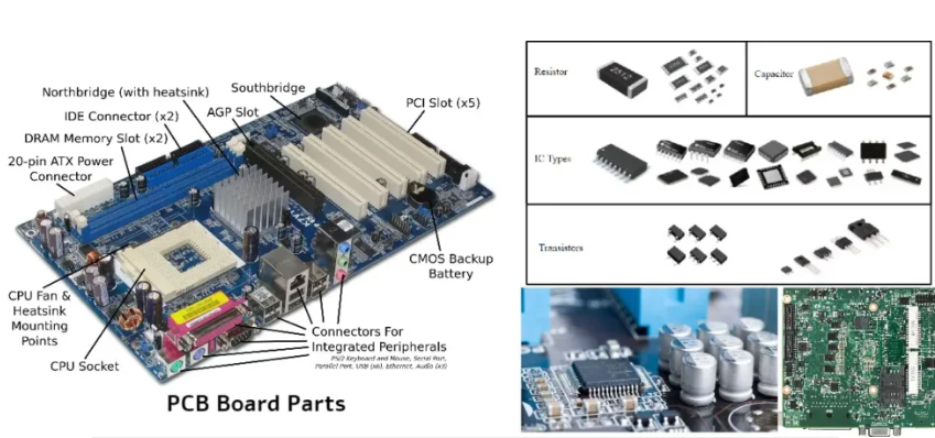
PCB module division and layout of key components
When talking about PCB EMC design, we cannot ignore the PCB module division and layout of key components. On the one hand, the relative position and direction of certain frequency generating devices, drivers, power modules, filter devices, etc. on the PCB will have a huge impact on the emission and reception of electromagnetic fields. On the other hand, the quality of the above layout will directly affect the quality of wiring.
Division by function
Various circuit modules implement different functions, such as clock circuits; amplifier circuits; drive circuits; A/D, D/A conversion circuits; I/O circuits, switching power supplies, filter circuits, etc. A complete design may include circuit modules with multiple functions. When designing PCB, we can divide the entire circuit into modules according to the signal flow direction. This ensures the rationality of the entire layout, achieves a short overall wiring path, and the modules are not intertwined, reducing the possibility of mutual interference between modules.
Division by frequency
Circuit modules can be divided according to the operating frequency and rate of the signal: high, medium, and low are gradually expanded and not intertwined.
Division by signal type
According to the signal type, it can be divided into two parts: digital circuit and analog circuit. In order to reduce the interference of digital circuits on analog circuits, so that they can coexist peacefully and achieve compatibility, different areas need to be defined for them during PCB layout, and necessary isolation should be performed in space to reduce mutual coupling. For digital-analog conversion circuits, such as A/D and D/A conversion circuits, they should be placed at the junction of digital circuits and analog circuits. The direction of device placement should be based on the flow of signals, so that the signal leads are as short as possible, and the pins of the analog part are located above the analog ground, and the pins of the digital part are located above the digital ground.
Comprehensive layout
One principle of circuit layout is that the key high-speed signal routing should be as short as possible according to the signal flow relationship, and secondly, the neatness and beauty of the circuit board should be considered. The clock signal should be as short as possible. If the clock routing cannot be shortened, shielded ground wires should be added on both sides of the clock line. Shielding measures should also be considered for more sensitive signal lines. The clock circuit has a large external radiation, which will have a great impact on some sensitive circuits, especially analog circuits. Therefore, the clock circuit should be kept away from other irrelevant circuits during circuit layout; in order to prevent the external radiation of the clock signal, the clock circuit should generally be kept away from the I/O circuit and cable connector. Low-frequency digital I/O circuits and analog I/O circuits should be placed close to the connectors, and clock circuits, high-speed circuits, and memory devices are often placed at the innermost part of the circuit board (away from the handle); medium and low-speed logic circuits are generally placed in the middle of the circuit board; if there are A/D and D/A circuits, they are generally placed in the middle of the circuit board.