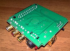
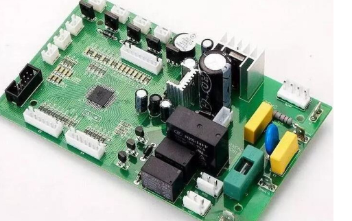
PCB multilayer circuit board protection technology
The protection technology that can be used on the PCB multilayer circuit board consists of three levels: components, circuit boards, and system devices.
1.Component level protection
Component level protection is to prevent ESD from coupling to circuits that are more sensitive to interference. Common transient suppression devices and filter devices are used for protection.
The use of transient suppression devices mainly depends on several main parameters: sensitivity, response voltage threshold, and response time: sensitivity determines whether the device can protect a certain level of interference; the response voltage threshold determines the circuit position where the device can play a protective role; the response time determines the effect after protection. The shorter the response time, the better the protection effect.
Filter devices mainly depend on two main links: frequency and placement position: frequency determines whether it can protect the circuit to be protected; placement position determines the protection effect. It is most beneficial to filter the interference before it enters the system, which can prevent the interference from re-radiating inside the system.
2.Circuit board level protection
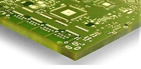
Generally speaking, multilayer printed circuit boards have a fixed ground layer, so their protection ability is better than that of single-layer and double-layer boards. Let the ground layer be as close to the wiring layer as possible. Such an arrangement can use ESD coupling to the low-impedance ground layer, which can significantly reduce the ESD energy reaching the signal line. You can refer to the following rules for design:
- Reduce the loop area. Both the signal line loop and the power supply loop need to be paid attention to;
- The power layer and the ground layer are arranged close to each other. This arrangement is more common and can play a good role in absorbing interference and suppressing radiation;
- Try to shorten the wiring length. Due to the fixed ground layer and power layer of the multilayer board, the placement and wiring of the devices are relatively free. Shortening the wiring length can not only reduce the intrusion of external interference, but also reduce the radiation interference of high-frequency signal lines to surrounding devices;
- Components with similar functions should be kept as close as possible. These devices are basically the same in terms of interference protection. Close layout can better concentrate targeted protection and unified treatment;
- The signal line is as close to the ground line, ground plane and corresponding circuit as possible;
- The transient suppression device used for protection is connected to the shell ground as directly as possible. This is because ESD will generate a large amount of current. The large current entering the system ground plane can cause serious ground rebound and even damage the components.
- When the PCB board is stacked, the connecting device should maintain enough ground pins. Sufficient ground pins can effectively reduce the ground impedance, reduce the mutual interference, and maintain the stable operation of the system.
- System device level protection
For the entire device, when the internal components and PCB board layers have been fixed, the protection of the entire system is very critical. You can refer to the following rules for design:
- Completely shield components and circuits that are sensitive to ESD radiation. Multi-point grounding through the shielding shell can provide a low-impedance channel for the absorbed ESD current. Circuits that cannot be ice-walled need to be effectively insulated, which has a certain protective effect on direct discharge and radiation coupling;
- The connecting cables inside the device should be kept away from buttons, gaps, etc. as much as possible to prevent interference from entering and affecting the entire system;
- Add interference suppression protection devices to each input and output interface. These places are often prone to static electricity due to direct contact and need to be protected. The protection devices are only based on the interface;
- The connection to the device shell ground should be as low impedance as possible;
- Special treatment is required for touch buttons to prevent static electricity generated by contact from being directly discharged to sensitive digital circuits;
- Use metal shell connectors;
- The tail line should be kept away from signal lines and I/O cables.