Pcb multilayer manufacturing process
Benefits Of Multilayer PCB Manufacturing
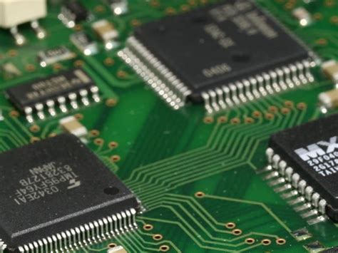
Multilayer printed circuit boards (PCBs) have become a cornerstone in modern electronics, offering numerous advantages over their single-layer and double-layer counterparts. The benefits of multilayer PCB manufacturing are manifold, encompassing aspects such as enhanced functionality, improved performance, and greater design flexibility. These advantages collectively contribute to the growing preference for multilayer PCBs in various high-tech applications.
One of the primary benefits of multilayer PCB manufacturing is the significant increase in circuit density.
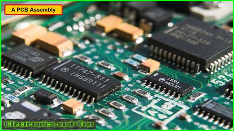
By stacking multiple layers of circuitry within a single board, designers can incorporate more components and connections in a compact space. This is particularly advantageous in the development of complex electronic devices, such as smartphones, laptops, and medical equipment, where space is at a premium. The ability to integrate more functionality into a smaller footprint not only saves space but also reduces the overall weight of the device, which is crucial for portable and wearable technologies.
In addition to increased circuit density, multilayer PCBs offer superior electrical performance.
The close proximity of the layers allows for shorter signal paths, which in turn reduces signal loss and electromagnetic interference (EMI). This results in faster signal transmission and improved signal integrity, making multilayer PCBs ideal for high-frequency applications and high-speed digital circuits. Furthermore, the use of multiple layers enables the implementation of advanced design techniques, such as controlled impedance and differential signaling, which are essential for maintaining signal quality in high-speed communication systems.
Another notable advantage of multilayer PCB manufacturing is the enhanced reliability and durability of the final product.
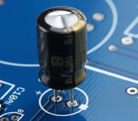
The multiple layers are bonded together using high-quality materials and advanced manufacturing processes, resulting in a robust and stable structure. This increased structural integrity makes multilayer PCBs more resistant to environmental stressors, such as temperature fluctuations, humidity, and mechanical vibrations. Consequently, devices that utilize multilayer PCBs tend to have longer lifespans and require less frequent maintenance, which is particularly beneficial in critical applications like aerospace, automotive, and industrial control systems.
Moreover, multilayer PCBs offer greater design flexibility, allowing engineers to create more sophisticated and intricate circuit layouts.
The additional layers provide ample routing space for complex interconnections, enabling the implementation of advanced features and functionalities. This design flexibility also facilitates the integration of various components, such as microprocessors, memory modules, and power management systems, into a single board. As a result, multilayer PCBs can support a wide range of applications, from consumer electronics to advanced computing systems and beyond.
The benefits of multilayer PCB manufacturing extend to the production process as well.
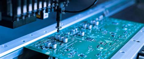
The use of automated manufacturing techniques, such as surface mount technology (SMT) and computer-aided design (CAD) tools, streamlines the production of multilayer PCBs, resulting in higher efficiency and lower production costs. Additionally, the ability to produce large volumes of multilayer PCBs with consistent quality and precision ensures that manufacturers can meet the demands of various industries while maintaining competitive pricing.
In conclusion, the advantages of multilayer PCB manufacturing are evident in the realms of circuit density, electrical performance, reliability, design flexibility, and production efficiency. These benefits have made multilayer PCBs an indispensable component in the development of modern electronic devices, driving innovation and enabling the creation of more advanced and compact technologies. As the demand for high-performance and miniaturized electronic devices continues to grow, the importance of multilayer PCB manufacturing will only become more pronounced, solidifying its role as a key enabler of technological progress.
Key Steps In Multilayer PCB Fabrication
The process of manufacturing multilayer printed circuit boards (PCBs) is a complex and intricate procedure that requires precision and attention to detail. It begins with the design phase, where engineers create a detailed blueprint of the PCB layout using specialized software. This design includes the placement of components, the routing of electrical connections, and the arrangement of multiple layers that will be stacked together. Once the design is finalized, it is converted into a format suitable for manufacturing, typically Gerber files, which contain all the necessary information for each layer of the PCB.
Following the design phase, the next step is the creation of the inner layers.
This involves transferring the design onto a copper-clad laminate using a process called photolithography. A photosensitive film, or photoresist, is applied to the laminate, and the design is then exposed onto the film using ultraviolet light. The exposed areas of the photoresist harden, while the unexposed areas remain soft and can be washed away, revealing the copper underneath. The exposed copper is then etched away using a chemical solution, leaving behind the desired circuit pattern.
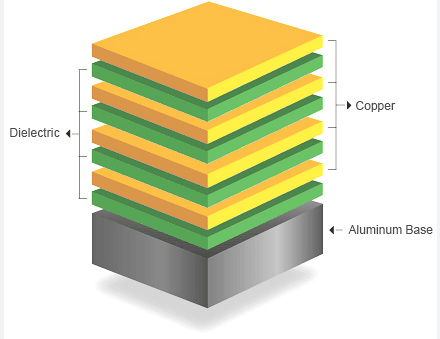
After the inner layers are created, they must be aligned and laminated together to form a single, cohesive unit.
This is achieved through a process called lamination, where the individual layers are stacked in the correct order and bonded together using heat and pressure. A layer of prepreg, a fiberglass material impregnated with resin, is placed between each copper layer to act as an adhesive. The entire stack is then placed in a press, where it is subjected to high temperatures and pressure to cure the resin and bond the layers together.
Once the lamination process is complete, the next step is drilling.
Holes are drilled through the PCB stack to create vias, which are used to connect the different layers electrically. These holes are drilled using precision machinery to ensure accuracy and consistency. After drilling, the holes are plated with copper to create a conductive path between the layers. This is done through a process called electroplating, where the PCB is submerged in a copper sulfate solution and an electric current is applied to deposit a thin layer of copper onto the walls of the holes.
Following the drilling and plating process, the outer layers of the PCB are created using a similar photolithography and etching process as the inner layers.
The outer layers are then coated with a solder mask, a protective layer that prevents solder from bridging between conductive traces and causing short circuits. The solder mask is applied using a screen-printing process and then cured using ultraviolet light.
The final steps in the multilayer PCB fabrication process involve the application of surface finishes and the addition of silkscreen markings.
Surface finishes, such as HASL (Hot Air Solder Leveling), ENIG (Electroless Nickel Immersion Gold), or OSP (Organic Solderability Preservative), are applied to the exposed copper areas to protect them from oxidation and improve solderability. Silkscreen markings, which include component labels, logos, and other identification marks, are printed onto the PCB using a screen-printing process.
In conclusion, the manufacturing of multilayer PCBs is a meticulous process that involves several key steps, including design, inner layer creation, lamination, drilling, plating, outer layer creation, solder mask application, and surface finishing. Each step requires precision and careful attention to detail to ensure the final product meets the required specifications and performs reliably in its intended application.
Common Challenges In Multilayer PCB Production
The production of multilayer printed circuit boards (PCBs) is a complex process that involves numerous steps, each of which presents its own set of challenges. One of the most significant challenges in multilayer PCB production is ensuring the precise alignment of the various layers. Misalignment can lead to electrical shorts or open circuits, which can render the entire board unusable. To mitigate this issue, manufacturers employ advanced alignment techniques and equipment, such as optical alignment systems, to ensure that each layer is perfectly aligned with the others.
Another common challenge is the management of thermal expansion.
Different materials used in the construction of PCBs, such as copper and various types of substrates, have different coefficients of thermal expansion. When the board is subjected to temperature changes during manufacturing or in its end-use environment, these differences can cause warping or delamination. To address this, manufacturers carefully select materials with compatible thermal properties and employ techniques such as pre-baking the substrates to stabilize them before assembly.
The drilling process also presents significant challenges.
Multilayer PCBs require numerous vias, or holes, to connect the different layers electrically. These vias must be drilled with extreme precision to avoid damaging the surrounding material and to ensure proper electrical connectivity. The use of high-speed, computer-controlled drilling machines helps to achieve the necessary precision, but even with advanced equipment, issues such as drill bit wear and material inconsistencies can lead to defects.
Copper plating is another critical step that can introduce challenges.
The vias and surface traces must be plated with copper to ensure good electrical conductivity. However, achieving uniform copper thickness can be difficult, especially in the small, deep vias required for high-density multilayer boards. Inconsistent plating can lead to weak connections and potential failure points. Manufacturers use techniques such as pulse plating and periodic reverse plating to improve the uniformity of the copper layer.
The etching process, which removes unwanted copper to create the desired circuit patterns, also poses challenges.
Over-etching can remove too much copper, leading to thin traces that are prone to breaking, while under-etching can leave excess copper that can cause shorts. Precise control of the etching process, including the concentration and temperature of the etching solution, is essential to achieve the desired results.
Solder mask application is another step that requires careful attention.
The solder mask protects the copper traces from oxidation and prevents solder bridges during component assembly. However, applying the solder mask evenly and accurately can be difficult, especially on boards with fine-pitch components and dense circuitry. Inaccurate solder mask application can lead to exposure of copper traces or covering of pads, both of which can cause assembly issues.
Finally, testing and inspection are crucial steps in the production of multilayer PCBs.
Given the complexity of these boards, thorough testing is necessary to ensure that all connections are intact and that there are no shorts or open circuits. Automated optical inspection (AOI) and electrical testing are commonly used to identify defects, but these methods must be carefully calibrated to detect all potential issues without generating false positives.
In conclusion, the production of multilayer PCBs involves navigating a series of intricate challenges, from layer alignment and thermal management to drilling, plating, etching, solder mask application, and final testing. Each step requires precise control and advanced techniques to ensure the production of reliable, high-quality boards. By understanding and addressing these challenges, manufacturers can produce multilayer PCBs that meet the stringent requirements of modern electronic devices.
Innovations In Multilayer PCB Technology
The manufacturing process of multilayer printed circuit boards (PCBs) has undergone significant innovations, driven by the increasing complexity and miniaturization of electronic devices. These advancements have not only enhanced the performance and reliability of PCBs but also expanded their applications across various industries. To understand these innovations, it is essential to delve into the intricacies of the multilayer PCB manufacturing process and the technological breakthroughs that have shaped it.
Initially, the process begins with the design phase, where engineers use sophisticated software to create detailed schematics and layouts.
This stage is crucial as it determines the electrical performance and physical structure of the PCB. Once the design is finalized, the manufacturing process commences with the preparation of the substrate material, typically made of fiberglass-reinforced epoxy resin, known as FR4. This material provides the necessary mechanical strength and electrical insulation.
Subsequently, the substrate is coated with a thin layer of copper, which serves as the conductive material for the circuit.
The copper layer is then subjected to a photolithographic process, where a photoresist material is applied and exposed to ultraviolet light through a mask that defines the circuit pattern. The exposed areas of the photoresist harden, while the unexposed areas remain soft and are subsequently removed, revealing the underlying copper. This step is followed by an etching process, where a chemical solution removes the unwanted copper, leaving behind the desired circuit pattern.
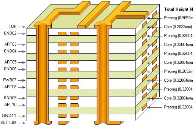
As the complexity of electronic devices increased, the need for multilayer PCBs became apparent.
These PCBs consist of multiple layers of circuitry stacked on top of each other, separated by insulating layers. The manufacturing of multilayer PCBs involves additional steps, such as the lamination process, where individual layers are bonded together under high pressure and temperature. This process ensures the structural integrity and electrical connectivity of the multilayer PCB.
One of the significant innovations in multilayer PCB technology is the development of advanced materials.
High-frequency laminates, for instance, have been introduced to cater to the demands of high-speed and high-frequency applications. These materials exhibit low dielectric loss and excellent thermal stability, making them ideal for applications such as telecommunications and radar systems. Additionally, the use of flexible and rigid-flex materials has enabled the design of PCBs that can bend and conform to complex shapes, expanding their applications in wearable devices and medical implants.
Another notable advancement is the implementation of advanced manufacturing techniques, such as laser drilling and direct imaging.
Laser drilling allows for the creation of microvias, which are tiny holes that connect different layers of the PCB. This technique offers higher precision and accuracy compared to traditional mechanical drilling, enabling the production of PCBs with finer features and higher density. Direct imaging, on the other hand, eliminates the need for photomasks by using laser or LED light to directly expose the photoresist. This method enhances the resolution and alignment accuracy, resulting in improved circuit performance.
Furthermore, the integration of automated inspection and testing systems has significantly improved the quality and reliability of multilayer PCBs.
Automated optical inspection (AOI) and automated X-ray inspection (AXI) systems are employed to detect defects such as misalignments, soldering issues, and internal voids. These systems ensure that only flawless PCBs proceed to the final assembly stage, reducing the risk of failures in the end product.
In conclusion, the innovations in multilayer PCB technology have revolutionized the manufacturing process, enabling the production of highly complex and reliable PCBs. The development of advanced materials, coupled with cutting-edge manufacturing techniques and automated inspection systems, has paved the way for the next generation of electronic devices. As technology continues to evolve, it is expected that further advancements in multilayer PCB manufacturing will continue to drive the progress of various industries, from telecommunications to healthcare and beyond.