Pcb multilayer press
Advantages Of PCB Multilayer Pressing Techniques
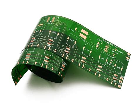
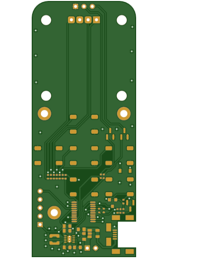
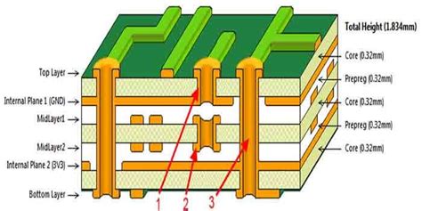
Multilayer PCB pressing techniques have revolutionized the electronics industry, offering numerous advantages that enhance the performance, reliability, and functionality of electronic devices. One of the primary benefits of multilayer PCB pressing is the significant increase in circuit density. By stacking multiple layers of circuitry within a single board, designers can create more complex and compact electronic devices. This is particularly advantageous in modern applications where space is at a premium, such as in smartphones, laptops, and other portable devices.
Another notable advantage is the improved electrical performance.
Multilayer PCBs allow for shorter and more direct electrical paths between components, which reduces the overall resistance and inductance. This results in faster signal transmission and better signal integrity, which is crucial for high-speed and high-frequency applications. Additionally, the ability to incorporate ground and power planes within the layers helps to minimize electromagnetic interference (EMI) and crosstalk, further enhancing the performance of the device.
The reliability of electronic devices is also significantly enhanced through multilayer PCB pressing techniques.
The use of multiple layers allows for redundant pathways, which can improve the overall durability and longevity of the device. In the event of a failure in one layer, the other layers can continue to function, thereby maintaining the integrity of the circuit. This redundancy is particularly important in critical applications such as aerospace, medical devices, and automotive systems, where reliability is paramount.
Furthermore, multilayer PCB pressing techniques offer greater design flexibility.
Designers can incorporate a variety of materials and components within the layers, allowing for the integration of different functionalities within a single board. This can lead to the development of more innovative and versatile electronic devices. For instance, designers can embed passive components such as resistors and capacitors within the layers, which can save space and reduce the overall size of the device.
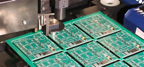
The manufacturing process of multilayer PCBs also benefits from pressing techniques.
The use of advanced pressing methods ensures that the layers are accurately aligned and bonded together, resulting in a high-quality and reliable final product. This precision is essential for maintaining the integrity of the electrical connections and ensuring the overall performance of the device. Additionally, the ability to produce multilayer PCBs in large quantities through automated pressing processes can lead to cost savings and increased production efficiency.
Moreover, multilayer PCB pressing techniques contribute to the overall sustainability of electronic devices.
By enabling the creation of more compact and efficient designs, these techniques can reduce the amount of raw materials required for production. This can lead to a decrease in electronic waste and a lower environmental impact. Additionally, the improved reliability and longevity of multilayer PCBs can extend the lifespan of electronic devices, further contributing to sustainability efforts.
In conclusion, the advantages of multilayer PCB pressing techniques are manifold, encompassing increased circuit density, improved electrical performance, enhanced reliability, greater design flexibility, and manufacturing benefits. These techniques have become indispensable in the development of modern electronic devices, driving innovation and enabling the creation of more advanced and efficient technologies. As the demand for smaller, faster, and more reliable electronic devices continues to grow, the importance of multilayer PCB pressing techniques will only become more pronounced, solidifying their role as a cornerstone of the electronics industry.
Common Challenges In Multilayer PCB Pressing And Solutions
Multilayer printed circuit boards (PCBs) are integral to modern electronics, offering enhanced functionality and compact design. However, the process of pressing these multilayer PCBs presents several challenges that can impact the quality and reliability of the final product. Understanding these common challenges and their solutions is crucial for manufacturers aiming to produce high-performance multilayer PCBs.
One of the primary challenges in multilayer PCB pressing is ensuring proper alignment of the layers.
Misalignment can lead to electrical shorts, open circuits, and overall malfunction of the PCB. To address this issue, manufacturers employ advanced registration systems that use optical or mechanical alignment techniques. These systems ensure that each layer is precisely aligned before pressing, thereby minimizing the risk of misalignment and improving the overall quality of the PCB.
Another significant challenge is the control of temperature and pressure during the pressing process.
Inconsistent temperature and pressure can result in incomplete bonding of the layers, leading to delamination or voids within the PCB. To mitigate this, manufacturers use sophisticated press machines equipped with precise temperature and pressure control mechanisms. These machines are capable of maintaining uniform conditions throughout the pressing cycle, ensuring that the layers bond correctly and form a solid, reliable structure.
The choice of materials also plays a critical role in the success of multilayer PCB pressing.
Different materials have varying thermal and mechanical properties, which can affect the pressing process. For instance, materials with high thermal expansion coefficients can cause warping or distortion during pressing. To overcome this, manufacturers carefully select materials that are compatible with each other and have similar thermal and mechanical properties. Additionally, they may use prepreg materials with specific resin formulations that enhance bonding and reduce the risk of defects.
Contamination is another challenge that can compromise the quality of multilayer PCBs.
Dust, debris, and other contaminants can become trapped between layers during pressing, leading to defects such as delamination or electrical shorts. To prevent contamination, manufacturers implement stringent cleanroom protocols and use advanced cleaning techniques to ensure that all materials and equipment are free from contaminants. This includes regular maintenance and cleaning of press machines, as well as the use of protective covers and cleanroom attire for personnel.
The complexity of multilayer PCBs also introduces challenges related to the design and layout of the layers.
Ensuring that the electrical connections between layers are correctly established requires meticulous design and precise execution. Manufacturers use advanced computer-aided design (CAD) software to create detailed layouts and simulate the pressing process. This allows them to identify potential issues and make necessary adjustments before actual production, thereby reducing the risk of defects and improving the overall reliability of the PCB.
In conclusion, the pressing of multilayer PCBs involves several challenges that can impact the quality and performance of the final product. However, by employing advanced alignment systems, precise temperature and pressure control mechanisms, careful material selection, stringent contamination prevention protocols, and meticulous design practices, manufacturers can effectively address these challenges. As a result, they can produce high-quality multilayer PCBs that meet the demanding requirements of modern electronic devices.
Innovations In Multilayer PCB Pressing Technology
The field of printed circuit board (PCB) manufacturing has witnessed significant advancements over the years, particularly in the realm of multilayer PCB pressing technology. This innovation is crucial for the development of complex electronic devices, as it allows for the integration of multiple layers of circuitry within a single board, thereby enhancing functionality and performance. The evolution of multilayer PCB pressing technology has been driven by the increasing demand for miniaturization, higher performance, and greater reliability in electronic devices.
One of the most notable innovations in multilayer PCB pressing technology is the development of advanced materials.
Traditional materials such as FR-4 have been supplemented with high-performance substrates that offer superior thermal and electrical properties. These advanced materials are essential for high-frequency applications and for devices that operate under extreme conditions. The use of such materials not only improves the overall performance of the PCBs but also extends their lifespan, making them more reliable for critical applications.
In addition to material advancements, the precision and accuracy of the pressing process have seen remarkable improvements.
Modern multilayer PCB presses are equipped with sophisticated control systems that ensure uniform pressure and temperature distribution across the entire board. This level of control is vital for achieving consistent quality and preventing defects such as delamination or misalignment of layers. The integration of real-time monitoring and feedback mechanisms further enhances the reliability of the pressing process, allowing manufacturers to detect and rectify issues promptly.
Another significant innovation is the adoption of automation in the multilayer PCB pressing process.
Automated systems have revolutionized the manufacturing landscape by reducing human error, increasing production speed, and ensuring consistent quality. These systems are capable of handling complex pressing cycles with high precision, thereby improving the overall efficiency of the production process. Moreover, automation facilitates the scalability of production, enabling manufacturers to meet the growing demand for multilayer PCBs without compromising on quality.
The environmental impact of PCB manufacturing has also been a focal point of recent innovations.
The pressing process, in particular, has seen the introduction of eco-friendly practices and materials. For instance, the use of lead-free solder and halogen-free laminates has become more prevalent, reducing the environmental footprint of PCB production. Additionally, advancements in waste management and recycling technologies have enabled manufacturers to minimize waste and recover valuable materials from discarded PCBs, contributing to a more sustainable manufacturing ecosystem.
Furthermore, the integration of advanced simulation and modeling tools has significantly enhanced the design and optimization of multilayer PCBs.
These tools allow engineers to simulate the pressing process and predict potential issues before actual production, thereby reducing the risk of defects and improving the overall yield. By leveraging these technologies, manufacturers can optimize the pressing parameters to achieve the desired performance characteristics while minimizing material usage and production costs.
In conclusion, the innovations in multilayer PCB pressing technology have been instrumental in meeting the evolving demands of the electronics industry. The advancements in materials, precision control, automation, environmental sustainability, and simulation tools have collectively contributed to the development of high-performance, reliable, and eco-friendly multilayer PCBs. As the industry continues to evolve, it is expected that these innovations will pave the way for even more sophisticated and efficient manufacturing processes, ultimately driving the next generation of electronic devices.
Step-By-Step Guide To Multilayer PCB Pressing Process
The process of pressing multilayer printed circuit boards (PCBs) is a critical step in the manufacturing of complex electronic devices. This intricate procedure involves several stages, each requiring meticulous attention to detail to ensure the final product meets the stringent standards of the electronics industry. Understanding the step-by-step guide to multilayer PCB pressing can provide valuable insights into the precision and care involved in creating these essential components.
Initially, the process begins with the preparation of the individual layers that will form the multilayer PCB.
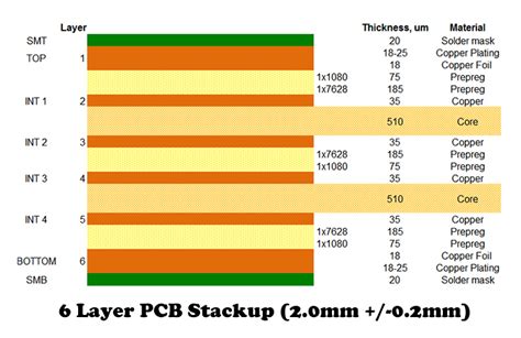
Each layer is typically composed of a thin sheet of copper foil laminated onto a substrate material, such as fiberglass-reinforced epoxy resin. These layers are meticulously cleaned and inspected to remove any contaminants that could affect the final product’s performance. Once the layers are prepared, they are coated with a thin layer of adhesive material, which will help bond them together during the pressing process.
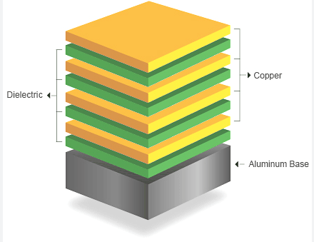
Following the preparation of the individual layers, the next step involves the alignment and stacking of these layers.
This is a crucial phase, as any misalignment can lead to defects in the final PCB. Advanced alignment tools and techniques are employed to ensure that each layer is precisely positioned relative to the others. The layers are then stacked in the correct order, with pre-preg sheets, which are layers of fiberglass pre-impregnated with resin, placed between them. These pre-preg sheets act as both an adhesive and an insulating material, helping to bond the layers together and providing electrical insulation between them.
Once the layers are stacked and aligned, the assembly is placed into a press.
The pressing process involves applying both heat and pressure to the stack, causing the adhesive material to flow and bond the layers together. The temperature and pressure must be carefully controlled to ensure that the adhesive cures properly without causing any damage to the layers. Typically, the press cycle involves a ramp-up phase, where the temperature and pressure are gradually increased, followed by a dwell phase, where they are held constant for a specified period, and finally a cool-down phase, where they are gradually decreased.
During the pressing process, it is essential to monitor the temperature and pressure closely to ensure that they remain within the specified ranges.
Any deviations can result in defects such as delamination, where the layers separate, or voids, where air pockets are trapped between the layers. Advanced monitoring and control systems are often used to maintain the required conditions and ensure the quality of the final product.
After the pressing process is complete, the multilayer PCB is removed from the press and allowed to cool to room temperature.
The cooled assembly is then subjected to a series of inspections and tests to verify its integrity and performance. These tests may include visual inspections, electrical tests, and X-ray inspections to check for any internal defects. Any defects identified during these inspections must be addressed before the PCB can be used in electronic devices.
In conclusion, the multilayer PCB pressing process is a complex and precise procedure that requires careful preparation, alignment, and control of temperature and pressure. Each step is critical to ensuring the final product meets the high standards required for modern electronic devices. By understanding this process, one can appreciate the level of expertise and attention to detail involved in creating these essential components.