PCB panel connection method/number of panels/process edge
PCB panelization is also a very important thing when designing PCB and mass producing PCB. It not only involves the quality standard of PCB circuit boards, but also affects the cost of PCB production. How to reasonably and effectively panelize while ensuring the quality of PCB circuit boards, so as to save raw materials, is a problem that production companies pay great attention to solving.
Panel connection method
PCB panel connection method has two connection methods, one is V-cut (as shown in Figure 3-30), and the other is stamp hole connection method (as shown in Figure 3-31).
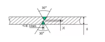
Figure 3-30 V-cut design of PCB
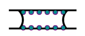
Figure 3-31 Design of stamp holes in PCB
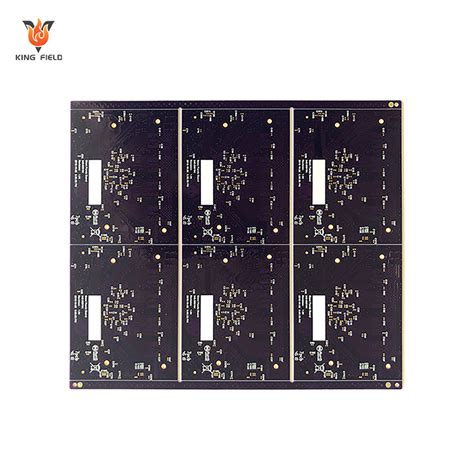
V-cut is generally suitable for PCB with rectangular shape. It has neat edges after separation and low processing cost. It is recommended to use it first, as shown in Figure 3-32;
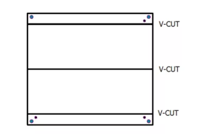
Figure 3-32 V-cut panel
Stamp holes are generally suitable for irregular panel layouts. For example, the “L” type frame structure of MID often uses the linking method of stamp holes for panel layout, as shown in Figure 3-33;
Number of panels
The size of the entire panel must be calculated based on the size of a single PCB board and cannot exceed the PCB The maximum size range (PCB panel length shall not exceed 250mm), and too many panels will affect the accuracy of the panel position and the patch accuracy. Generally, the main board of MID type is 2 panels, and the sub-boards of keypad and LCD board are not more than 6 panels. The sub-boards of special area are determined according to the specific situation.
Requirements for stamp hole link strips
In a PCB panel, the number of link strips should be appropriate, generally 2-3 link strips, so that the strength of the PCB meets the requirements of the production process and does not break easily.
As shown in Figure 3-34, when designing the link bar, it is generally necessary to design a length of 4-5mm, the hole is a non-metalized hole, the size is generally 0.3mm-0.5mm, and the spacing between the holes is 0.8-1.2mm;
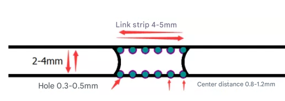
Figure 3-34 Design of link bar
Process edge
When the board is densely populated and the board edge space is limited, it is necessary to increase the process edge to be used for the transfer edge of the PCB board during SMT, generally 3-5mm. On the process edge, generally one positioning hole is added to each of the four corners, and optical positioning points are added to the three corners to strengthen the positioning of the machine, as shown in Figure 3-35.
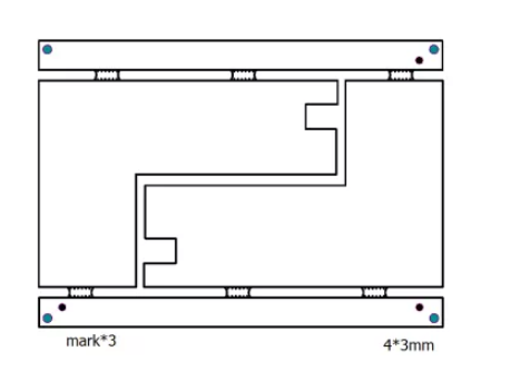
Figure 3-35 Design of process edge