PCB Panelization Techniques: Maximizing Efficiency and Cost-Effectiveness
Introduction to PCB Panelization
Printed Circuit Board (PCB) panelization is a critical manufacturing technique that involves arranging multiple PCB designs onto a single panel for production. This process offers numerous advantages, including reduced manufacturing costs, improved production efficiency, and enhanced handling during assembly. As electronics continue to shrink in size while growing in complexity, effective panelization has become increasingly important for both manufacturers and designers.
Panelization, also known as “step-and-repeat” or “arraying,” requires careful consideration of various factors such as board shape, component placement, routing requirements, and manufacturing constraints. When executed properly, panelization can significantly reduce material waste, minimize processing time, and improve overall product quality. This article explores the fundamental principles, techniques, and best practices for effective PCB panelization.
Basic Panelization Methods
1. V-Scoring (V-Groove)
V-scoring is one of the most common panelization techniques, particularly suitable for rectangular or square PCBs. This method involves creating V-shaped grooves on the top and bottom surfaces of the panel, leaving a thin layer of material (typically 1/3 of the board thickness) to hold the boards together. The main advantages of V-scoring include:
- Clean break edges after depaneling
- Minimal material waste between boards
- Cost-effective tooling requirements
- Suitable for high-volume production
The standard V-score angle is 30° or 45°, with the depth carefully calculated to ensure proper holding strength during manufacturing while allowing easy separation afterward. V-scoring works best for boards with straight edges and is less suitable for complex contours.
2. Tab Routing (Breakaway Tabs)
Tab routing, also known as breakaway tabs or mouse bites, involves routing out most of the material between boards while leaving small connecting tabs at regular intervals. These tabs typically contain several small drill holes (mouse bites) that weaken the connection for easier depaneling. Key characteristics include:
- Ideal for irregularly shaped PCBs
- Allows closer spacing of complex board outlines
- Provides more support during assembly than V-scoring
- Requires more post-processing for clean edges
Tab routing offers greater flexibility in panel layout compared to V-scoring but may leave small protrusions that require additional finishing. The number and size of tabs should be carefully determined based on board size and weight to ensure adequate support during manufacturing.
3. Perforated Panelization
Perforated panelization is a hybrid approach that combines elements of both V-scoring and tab routing. This method uses a series of small perforations along the separation line instead of continuous grooves or tabs. Benefits include:
- Smooth separation with minimal stress on components
- Reduced risk of board damage during depaneling
- Suitable for fragile or sensitive components
- Cleaner edges than standard tab routing
This technique is particularly useful for boards with components placed near the edges or those requiring very clean break lines. However, it may require specialized equipment and can be more expensive than standard methods.
Advanced Panelization Strategies
1. Mixed Technology Panelization
Modern electronics often combine various technologies on a single board, such as through-hole components, surface mount devices (SMD), and ball grid arrays (BGA). Mixed technology panelization considers:
- Different reflow requirements for components
- Wave soldering considerations for through-hole parts
- Thermal management across the panel
- Component height restrictions for assembly processes
Effective mixed technology panelization may involve creating separate zones within the panel or adjusting the layout to accommodate different manufacturing processes.
2. High-Density Interconnect (HDI) Panelization
HDI PCBs with microvias and fine pitch components require special panelization considerations:
- Tighter tolerances for registration and alignment
- Specialized depaneling methods to prevent microvia damage
- Consideration of laser drilling requirements
- More stringent cleanroom requirements for some processes
HDI panelization often employs modified tab routing with additional support structures to maintain dimensional stability during manufacturing.
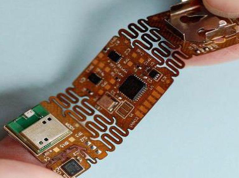
3. Flexible and Rigid-Flex Panelization
Flexible PCBs and rigid-flex designs present unique panelization challenges:
- Accounting for material shrinkage and expansion
- Special handling requirements during assembly
- Stress relief considerations for flex areas
- Unique depaneling methods for flexible materials
These boards often require specialized carrier systems or additional panel borders to maintain stability during manufacturing processes.
Design Considerations for Effective Panelization
1. Panel Size Optimization
Standard panel sizes vary by manufacturer but typically range from 18″×24″ to 21″×24″. Key optimization factors include:
- Maximizing board count per panel
- Minimizing material waste
- Considering equipment limitations
- Balancing panel size with handling requirements
Designers should consult with their manufacturers to determine the most cost-effective panel size for their specific project.
2. Fiducial Markers and Tooling Holes
Proper panelization requires accurate registration marks:
- Global fiducials for panel alignment
- Local fiducials for individual board alignment
- Standardized tooling holes for machine handling
- Clearance areas around fiducials
These features ensure precise component placement and reliable automated assembly processes.
3. Component Keep-Out Zones
Critical areas to consider:
- Board edges (typically 3-5mm for depaneling)
- V-score or tab routing areas
- Panel borders for handling
- Areas under clamping devices
Components placed too close to these zones may be damaged during manufacturing or depaneling.
4. Depaneling Method Selection
The choice of depaneling method affects many design decisions:
- Manual breaking (simple but inconsistent)
- Punching (fast but requires tooling)
- Routing (precise but slower)
- Laser cutting (high precision but expensive)
The selected depaneling method should be considered early in the design phase to ensure proper panel layout.
Manufacturing and Assembly Considerations
1. Panel Strength and Stability
The panel must maintain integrity throughout:
- Solder paste application
- Component placement
- Reflow processes
- Handling and transportation
This may require additional support structures or breakaway tabs in weak areas.
2. Thermal Management
Large panels can experience uneven heating:
- Thermal mass distribution
- Warpage prevention
- Consistent reflow profiles
- Heat dissipation considerations
Proper panel design can minimize thermal-related defects during soldering processes.
3. Testing and Inspection
Panelization affects testing strategies:
- Flying probe test access
- Bed-of-nails fixture design
- Automated optical inspection (AOI) requirements
- Boundary scan considerations
Test access points should be included in the panel design to facilitate quality control.
Cost Optimization Through Panelization
1. Material Utilization
Effective panelization can significantly reduce costs by:
- Maximizing board count per panel
- Minimizing scrap material
- Reducing handling per unit
- Optimizing raw material usage
Even small improvements in material utilization can lead to substantial savings in high-volume production.
2. Labor Efficiency
Panelization reduces per-unit labor costs through:
- Batch processing of multiple boards
- Reduced handling operations
- Automated assembly advantages
- Streamlined testing procedures
3. Tooling and Setup Costs
Well-designed panels can minimize:
- Fixture requirements
- Setup time per unit
- Tool wear and maintenance
- Changeover time between jobs
Emerging Trends in PCB Panelization
1. Smart Panelization Software
Advanced software tools now offer:
- Automated optimal layout algorithms
- Design rule checking for panelization
- 3D visualization of assembled panels
- Manufacturing process simulation
These tools help designers create more efficient panels while avoiding common pitfalls.
2. Laser Depaneling Technology
Laser systems provide:
- Precise, clean cuts
- No mechanical stress on boards
- Ability to cut complex shapes
- Minimal heat-affected zones
While currently more expensive than traditional methods, laser depaneling is becoming more accessible for high-value PCBs.
3. Sustainable Panelization
Eco-conscious practices include:
- Material-efficient layouts
- Recyclable panel materials
- Reduced chemical usage
- Energy-efficient manufacturing
Sustainable panelization not only benefits the environment but can also reduce costs in some cases.
Best Practices for PCB Panelization
- Early Collaboration: Engage with your manufacturer during the design phase to optimize panelization.
- Standardization: Use standard panel sizes when possible to avoid special setup charges.
- Balance: Distribute board layouts evenly across the panel to prevent warping and ensure consistent processing.
- Clear Documentation: Provide detailed panel drawings with all critical dimensions and requirements.
- Prototype: Test panel designs with small runs before committing to full production.
- Consider the Entire Process: Account for all manufacturing steps from fabrication through final assembly.
- Review and Iterate: Continuously improve panel designs based on production feedback.
Conclusion
Effective PCB panelization is both an art and a science, requiring careful consideration of design requirements, manufacturing capabilities, and cost factors. By understanding and applying the various panelization techniques and principles outlined in this article, designers and manufacturers can significantly improve production efficiency, reduce costs, and enhance product quality.
As PCB technology continues to evolve with higher densities, more complex components, and new materials, panelization techniques must similarly advance. Staying informed about the latest developments in panelization technology and methodologies will remain crucial for maintaining competitiveness in the electronics manufacturing industry.
The most successful panelization strategies result from close collaboration between designers and manufacturers, balancing the sometimes competing demands of design intent, manufacturability, and cost efficiency. By viewing panelization as an integral part of the design process rather than an afterthought, companies can realize significant benefits throughout the product lifecycle.