PCB Potting Compound: A Comprehensive Guide
Introduction
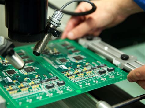
Printed Circuit Boards (PCBs) are the backbone of modern electronic devices, providing mechanical support and electrical connections between components. However, PCBs are often exposed to harsh environmental conditions such as moisture, dust, chemicals, and mechanical stress, which can lead to failure. To enhance durability and reliability, PCB potting compounds are widely used to encapsulate and protect electronic assemblies.
This article explores PCB potting compounds in detail, covering their types, benefits, applications, selection criteria, and future trends.
1. What is PCB Potting Compound?
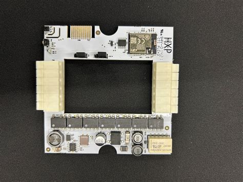
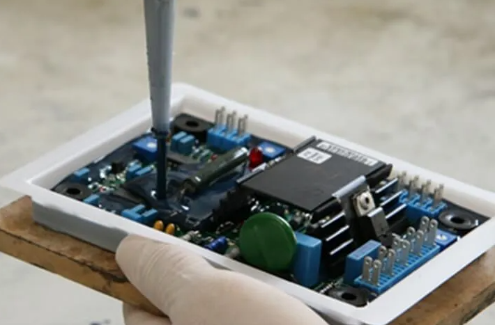
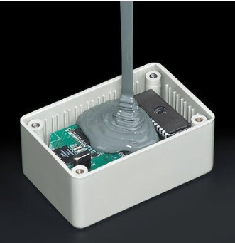
PCB potting compound is a liquid resin that is poured or injected over electronic components and circuits to form a solid protective layer after curing. This process, known as potting, seals the PCB from external factors, improving mechanical strength, thermal management, and electrical insulation.
Key Characteristics of Potting Compounds
- Chemical Resistance – Protects against solvents, acids, and alkalis.
- Thermal Stability – Maintains performance under high temperatures.
- Electrical Insulation – Prevents short circuits and leakage currents.
- Mechanical Protection – Absorbs shocks and vibrations.
- Moisture & Corrosion Resistance – Shields against humidity and oxidation.
2. Types of PCB Potting Compounds
Different potting materials are used based on application requirements. The most common types include:
A. Epoxy Potting Compounds
Epoxy resins are widely used due to their excellent adhesion, chemical resistance, and mechanical strength. They are ideal for high-stress environments.
Advantages:
✔ High thermal and chemical resistance
✔ Strong mechanical protection
✔ Low shrinkage during curing
Disadvantages:
✖ Rigid after curing (may crack under extreme stress)
✖ Longer curing time compared to silicones
B. Silicone Potting Compounds
Silicones offer flexibility and high-temperature stability, making them suitable for applications requiring thermal cycling resistance.
Advantages:
✔ Excellent flexibility and elasticity
✔ High thermal stability (-50°C to 200°C)
✔ Good moisture resistance
Disadvantages:
✖ Lower mechanical strength than epoxy
✖ More expensive
C. Polyurethane Potting Compounds
Polyurethane (PU) potting compounds provide a balance between flexibility and toughness, ideal for shock absorption.
Advantages:
✔ Good vibration damping
✔ Resistant to abrasion and impact
✔ Faster curing than epoxy
Disadvantages:
✖ Lower thermal resistance than epoxy/silicone
✖ Susceptible to moisture absorption
D. UV-Curable Potting Compounds
These compounds cure rapidly under UV light, making them suitable for fast production processes.
Advantages:
✔ Instant curing (seconds to minutes)
✔ Low energy consumption
Disadvantages:
✖ Limited depth of cure (requires UV exposure)
✖ Not suitable for opaque assemblies
3. Benefits of PCB Potting
Potting enhances PCB performance in multiple ways:
A. Environmental Protection
- Prevents moisture, dust, and chemical ingress.
- Reduces oxidation and corrosion of metal traces.
B. Mechanical Stability
- Absorbs vibrations and shocks (critical in automotive and aerospace applications).
- Reinforces delicate components (e.g., capacitors, connectors).
C. Electrical Insulation
- Prevents arcing and short circuits in high-voltage applications.
- Improves dielectric strength.
D. Thermal Management
- Some thermally conductive potting compounds dissipate heat efficiently.
- Reduces thermal stress on components.
E. Tamper Resistance
- Encapsulation makes reverse engineering difficult, enhancing security.

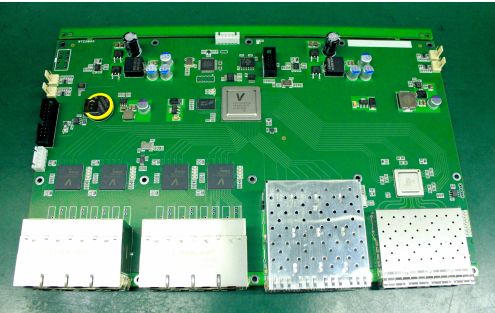
4. Applications of PCB Potting Compounds
Potting compounds are used across various industries:
A. Automotive Electronics
- Protects ECUs (Engine Control Units), sensors, and battery management systems from heat and vibration.
B. Industrial Electronics
- Shields motor drives, power supplies, and control systems from harsh factory conditions.
C. Consumer Electronics
- Used in LED drivers, power adapters, and smart devices to enhance durability.
D. Aerospace & Defense
- Ensures reliability in avionics, radar systems, and military-grade electronics.
E. Medical Devices
- Provides biocompatible encapsulation for implants and diagnostic equipment.
F. Renewable Energy Systems
- Protects solar inverters and wind turbine controllers from environmental exposure.
5. How to Select the Right Potting Compound?
Choosing the best potting material depends on several factors:
A. Operating Environment
- Temperature Range: Silicone for extreme temperatures, epoxy for high thermal resistance.
- Chemical Exposure: Epoxy for harsh chemicals, polyurethane for moderate conditions.
B. Mechanical Requirements
- Flexibility Needed? Silicone or polyurethane for dynamic stress.
- Impact Resistance? Polyurethane or toughened epoxy.
C. Electrical Properties
- Dielectric Strength: Epoxy for high-voltage insulation.
- Frequency of Operation: Low-loss materials for RF applications.
D. Curing Process
- Fast Production? UV-curable or fast-cure polyurethane.
- Deep Potting? Two-part epoxy or silicone for deep encapsulation.
E. Cost Considerations
- Epoxy is cost-effective for rigid applications.
- Silicone is pricier but offers superior flexibility.
6. Future Trends in PCB Potting Technology
The potting compound industry is evolving with new advancements:
A. Eco-Friendly Formulations
- Bio-based resins and low-VOC (Volatile Organic Compound) materials are gaining popularity.
B. Enhanced Thermal Conductivity
- Nano-filled compounds for better heat dissipation in high-power electronics.
C. Self-Healing Potting Materials
- Polymers that repair minor cracks autonomously, extending PCB lifespan.
D. Smart Encapsulation
- Integration of sensors within potting compounds for real-time monitoring.
E. 3D Printing of Potting Structures
- Customized encapsulation using additive manufacturing techniques.

7. Conclusion
PCB potting compounds play a crucial role in enhancing the durability, reliability, and performance of electronic assemblies. The choice of potting material—whether epoxy, silicone, polyurethane, or UV-curable—depends on the specific application requirements.
As technology advances, potting compounds are becoming more sophisticated, offering improved thermal management, environmental sustainability, and smart functionalities. Engineers must carefully evaluate factors like mechanical stress, thermal conditions, and electrical properties to select the optimal potting solution.
By leveraging the right potting techniques, manufacturers can ensure longer-lasting, high-performance PCBs across industries—from automotive and aerospace to medical and renewable energy systems.