PCB Power Supply Design: Principles, Challenges, and Best Practices
Introduction
Power supply design is a critical aspect of printed circuit board (PCB) development, influencing the performance, reliability, and efficiency of electronic systems. Whether designing a simple linear regulator or a complex switch-mode power supply (SMPS), engineers must consider factors such as voltage regulation, noise suppression, thermal management, and electromagnetic compatibility (EMC). This article explores the fundamental principles of PCB power supply design, common challenges, and best practices to ensure optimal performance.
1. Fundamentals of PCB Power Supply Design
1.1 Types of Power Supplies
Power supplies in PCBs can be broadly categorized into two types:
- Linear Regulators: These provide stable output voltage with low noise but are inefficient for high current applications due to heat dissipation.
- Switch-Mode Power Supplies (SMPS): These are highly efficient but generate more noise, requiring careful filtering and layout design.
1.2 Key Design Considerations
- Voltage Regulation: Ensuring a stable output voltage despite input fluctuations.
- Efficiency: Minimizing power losses to reduce heat generation.
- Noise and Ripple: Managing high-frequency switching noise in SMPS designs.
- Thermal Management: Preventing overheating through proper component placement and heat sinking.
- EMC/EMI Compliance: Reducing electromagnetic interference to meet regulatory standards.
2. Power Supply Topologies for PCBs
Different power supply topologies are used based on application requirements:
2.1 Buck Converters (Step-Down)
- Reduces input voltage to a lower output voltage.
- High efficiency but requires proper inductor and capacitor selection.
2.2 Boost Converters (Step-Up)
- Increases input voltage to a higher output voltage.
- Used in battery-powered devices where voltage needs to be stepped up.
2.3 Buck-Boost Converters
- Can step up or step down voltage as needed.
- Useful in applications with varying input voltages.
2.4 Low-Dropout (LDO) Regulators
- Provides clean, low-noise output but with higher power dissipation.
- Ideal for noise-sensitive analog circuits.
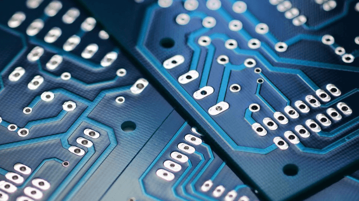
3. PCB Layout Considerations for Power Supplies
A well-designed PCB layout is crucial for minimizing noise, reducing losses, and ensuring thermal stability.
3.1 Component Placement
- Place power components (inductors, capacitors, regulators) close to each other to minimize parasitic inductance and resistance.
- Keep high-current traces short and wide to reduce voltage drops.
3.2 Grounding Techniques
- Use a star grounding approach to avoid ground loops.
- Separate analog and digital ground planes to minimize noise coupling.
3.3 Trace Routing
- Use thick traces for high-current paths (e.g., 20-50 mils for 1A current).
- Avoid sharp angles in traces to prevent impedance discontinuities.
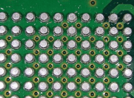
3.4 Decoupling and Filtering
- Place decoupling capacitors (e.g., 0.1µF, 10µF) near IC power pins.
- Use ferrite beads and LC filters to suppress high-frequency noise.
3.5 Thermal Management
- Use thermal vias under high-power components to dissipate heat.
- Consider copper pours or heat sinks for components like MOSFETs and regulators.
4. Common Challenges in PCB Power Supply Design
4.1 Switching Noise in SMPS
- High-frequency switching introduces noise, which can affect sensitive analog circuits.
- Solution: Use proper filtering, shielding, and layout separation.
4.2 Voltage Drop and IR Losses
- Long, thin traces increase resistance, leading to voltage drops.
- Solution: Optimize trace width and use power planes where possible.
4.3 EMI and EMC Issues
- Switching regulators can radiate electromagnetic interference.
- Solution: Follow proper grounding, shielding, and component placement guidelines.
4.4 Thermal Runaway
- Excessive heat can degrade components and reduce lifespan.
- Solution: Implement thermal vias, heat sinks, and proper airflow.
5. Best Practices for Optimizing PCB Power Supply Design
5.1 Simulation and Prototyping
- Use SPICE simulations to analyze power supply behavior before fabrication.
- Test prototypes under different load conditions to validate performance.
5.2 Component Selection
- Choose inductors and capacitors with low equivalent series resistance (ESR).
- Select MOSFETs and diodes with appropriate voltage/current ratings.
5.3 Feedback Loop Stability
- Ensure proper compensation in SMPS designs to avoid oscillations.
- Use phase margin analysis to verify stability.
5.4 Compliance with Industry Standards
- Follow IPC-2221 for general PCB design guidelines.
- Ensure compliance with EMI/EMC standards (e.g., FCC, CE).
5.5 Testing and Validation
- Measure ripple and noise using an oscilloscope.
- Perform thermal imaging to identify hotspots.
6. Future Trends in PCB Power Supply Design
- GaN and SiC Devices: Gallium Nitride (GaN) and Silicon Carbide (SiC) transistors enable higher efficiency and smaller form factors.
- Integrated Power Modules: Combining power stages into single ICs simplifies design.
- AI-Assisted Optimization: Machine learning tools can help optimize power supply layouts for efficiency and thermal performance.
Conclusion
Designing an efficient and reliable PCB power supply requires careful consideration of topology, component selection, layout, and thermal management. By following best practices—such as minimizing noise, optimizing trace routing, and ensuring proper grounding—engineers can develop power supplies that meet performance and regulatory requirements. As power electronics evolve, emerging technologies like GaN and advanced simulation tools will further enhance power supply design capabilities.
.


