PCB Press-Fit Hole Technology: A Comprehensive Guide
Abstract
Press-fit technology has become a critical assembly method in printed circuit board (PCB) manufacturing, offering a reliable, solderless solution for component mounting. This article explores the fundamentals of PCB press-fit hole technology, including its advantages, design considerations, process parameters, and common challenges. By understanding the key aspects of press-fit connections, engineers can optimize their PCB designs for improved mechanical stability and electrical performance.
1. Introduction to Press-Fit Technology
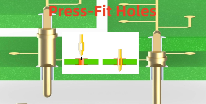
Press-fit technology involves the mechanical insertion of a compliant pin into a plated through-hole (PTH) on a PCB, creating a secure electrical and mechanical connection without soldering. This method is widely used in high-reliability applications such as automotive, aerospace, and industrial electronics, where vibration resistance and long-term durability are essential.
1.1 Advantages of Press-Fit Connections
- Solderless Assembly: Eliminates thermal stress and soldering defects.
- High Mechanical Stability: Provides strong retention force, ideal for high-vibration environments.
- Reusability: Components can be removed and reinserted without damaging the PCB.
- Improved Thermal Performance: Better heat dissipation compared to soldered joints.
- Compatibility with High-Current Applications: Low contact resistance ensures reliable power delivery.
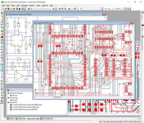
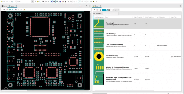
2. PCB Press-Fit Hole Design Considerations
Designing a PCB for press-fit applications requires careful attention to hole size, plating thickness, and material selection.
2.1 Hole Diameter and Tolerance
The press-fit hole diameter must be slightly smaller than the pin diameter to ensure interference fit. Typical tolerances range from ±0.05 mm to ±0.10 mm. The recommended hole size depends on the pin’s compliance and the PCB material.
2.2 Plating Thickness
Adequate copper plating ensures mechanical strength and electrical conductivity:
- Standard Thickness: 25–35 μm (1 oz/ft²)
- High-Reliability Applications: Up to 50 μm (2 oz/ft²)
2.3 PCB Material Selection
- FR-4: Most common, suitable for moderate mechanical stress.
- High-Tg Materials: Preferred for high-temperature applications.
- Metal-Core PCBs: Used in power electronics for enhanced thermal dissipation.
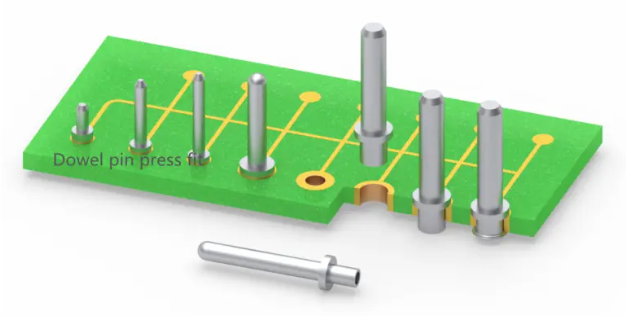
3. Press-Fit Pin Types and Compliance
Press-fit pins come in various designs, each offering different levels of compliance and retention force.
3.1 Common Press-Fit Pin Designs
- Eye-of-the-Needle (EON) Pins:
- Most widely used due to excellent retention and compliance.
- Features a split cylindrical design for elastic deformation.
- Solid Pins:
- Used for high-current applications.
- Requires precise hole sizing to avoid PCB damage.
- Crowned Pins:
- Provides multiple contact points for improved reliability.
3.2 Compliance and Insertion Force
The pin’s compliance determines the required insertion force and retention strength. Engineers must balance:
- Insertion Force: Typically 20–100 N per pin.
- Retention Force: Should exceed 50 N for vibration resistance.
4. Press-Fit Assembly Process
The press-fit assembly process involves precise control of insertion force, alignment, and inspection.
4.1 Insertion Methods
- Manual Press-Fit: Suitable for prototyping and low-volume production.
- Semi-Automatic Presses: Used in medium-volume manufacturing.
- Fully Automated Systems: High-speed insertion for mass production.
4.2 Process Parameters
- Insertion Speed: 1–10 mm/sec to avoid excessive stress.
- Alignment Accuracy: ±0.1 mm to prevent pin bending.
- Post-Insertion Inspection: Visual, mechanical pull tests, and electrical continuity checks.
5. Challenges and Solutions in Press-Fit Technology
5.1 Common Issues
- PCB Cracking: Caused by excessive insertion force or poor hole design.
- Poor Electrical Contact: Due to insufficient plating or contamination.
- Pin Deformation: Misalignment during insertion can bend pins.
5.2 Mitigation Strategies
- Optimized Hole Design: Use simulation tools to validate interference fit.
- Surface Finish Selection: ENIG (Electroless Nickel Immersion Gold) or hard gold for better conductivity.
- Process Control: Implement automated force monitoring during insertion.
6. Applications of Press-Fit Technology
Press-fit connections are used in:
- Automotive ECUs: Vibration-resistant connections for engine control units.
- Aerospace Electronics: High-reliability avionics systems.
- Power Electronics: Busbars and high-current connectors.
- Telecommunications: Backplane connectors in server systems.
7. Future Trends in Press-Fit Technology
- Miniaturization: Smaller press-fit pins for high-density PCBs.
- Advanced Materials: Composite pins for improved durability.
- Industry 4.0 Integration: AI-based quality control in press-fit assembly.
8. Conclusion
PCB press-fit hole technology offers a robust alternative to soldering, particularly in high-stress environments. By optimizing hole design, plating, and insertion processes, manufacturers can achieve reliable, long-lasting connections. As electronic assemblies become more complex, press-fit technology will continue to evolve, enabling next-generation PCB designs.