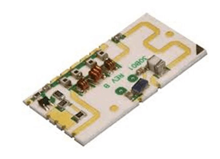
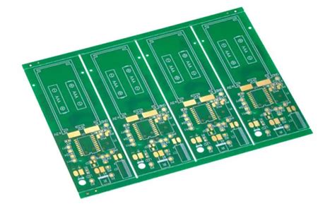
Pcb prototype 4 layer
Design Tips For A Successful 4-Layer PCB Prototype
Designing a successful 4-layer PCB prototype requires meticulous planning and a deep understanding of the intricacies involved in multi-layer PCB design. The complexity of a 4-layer PCB, compared to its single or double-layer counterparts, necessitates a more strategic approach to ensure optimal performance and reliability.
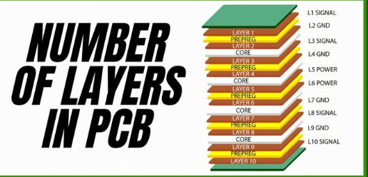
To begin with, it is essential to comprehend the fundamental structure of a 4-layer PCB, which typically consists of two internal layers sandwiched between two external layers. This configuration allows for enhanced signal integrity, reduced electromagnetic interference (EMI), and improved power distribution.
One of the primary considerations in designing a 4-layer PCB prototype is the layer stack-up.
The stack-up arrangement significantly influences the electrical performance and manufacturability of the PCB. A common stack-up configuration includes a signal layer, a ground plane, a power plane, and another signal layer. This arrangement helps in minimizing signal crosstalk and ensuring a stable reference plane for signal integrity. It is advisable to place the ground plane adjacent to the signal layers to provide a low-impedance return path for high-speed signals, thereby reducing EMI.
Transitioning to the topic of trace routing, it is crucial to adopt a systematic approach to avoid potential issues such as signal interference and impedance mismatches.
High-speed signal traces should be routed on the outer layers, while the inner layers can be reserved for power and ground planes. This practice not only simplifies the routing process but also enhances signal integrity by providing a consistent reference plane. Additionally, maintaining a uniform trace width and spacing is vital to ensure controlled impedance, which is particularly important for high-frequency signals.
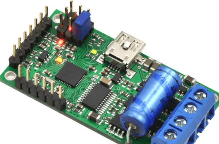
Another critical aspect to consider is the placement of components.
Strategic component placement can significantly impact the overall performance and manufacturability of the PCB. It is recommended to group components with similar functions together and place them in close proximity to minimize trace lengths and reduce signal delay. Furthermore, sensitive components such as oscillators and analog circuits should be isolated from high-speed digital circuits to prevent noise coupling and signal degradation.
Thermal management is another key factor in the design of a 4-layer PCB prototype.
The increased density of components and traces in a multi-layer PCB can lead to higher heat generation, which, if not managed properly, can affect the performance and longevity of the PCB. Implementing thermal vias, heat sinks, and proper ventilation can help dissipate heat effectively. Additionally, using thicker copper layers for power and ground planes can enhance heat dissipation and improve current-carrying capacity.
In addition to these design considerations, it is essential to perform thorough design rule checks (DRC) and electrical rule checks (ERC) to identify and rectify potential issues before proceeding to fabrication. Utilizing advanced PCB design software with built-in DRC and ERC capabilities can streamline this process and ensure compliance with industry standards.
Finally, collaboration with a reputable PCB manufacturer is crucial to the success of your 4-layer PCB prototype.
Engaging with the manufacturer early in the design process can provide valuable insights into manufacturability constraints and help optimize the design for cost-effective production. By adhering to these design tips and maintaining a collaborative approach, you can achieve a successful 4-layer PCB prototype that meets your performance and reliability requirements.
Common Challenges In 4-Layer PCB Prototyping And How To Overcome Them
Prototyping a 4-layer printed circuit board (PCB) is a complex process that presents several challenges, even for experienced engineers. Understanding these challenges and knowing how to address them is crucial for ensuring the success of your project. One of the primary difficulties in 4-layer PCB prototyping is managing the increased complexity compared to simpler, single or double-layer boards. The additional layers provide more routing options and can support more complex circuits, but they also require meticulous planning and design to avoid issues such as signal interference and crosstalk.
To overcome this, it is essential to use advanced design software that can handle multi-layer PCB layouts.
These tools often come with features that help in visualizing the different layers and their interactions, making it easier to identify potential problems early in the design phase. Additionally, adhering to best practices in PCB design, such as maintaining consistent trace widths and spacing, can significantly reduce the risk of signal integrity issues.
Another common challenge is thermal management.
With more layers, there is an increased likelihood of heat buildup, which can affect the performance and longevity of the components. Effective thermal management strategies, such as incorporating thermal vias and using materials with good thermal conductivity, are vital. Thermal vias help in dissipating heat by providing a path for it to travel from the hot components to the cooler areas of the board. Moreover, selecting materials with high thermal conductivity can aid in spreading the heat more evenly across the board, thereby preventing hotspots.
The manufacturing process for 4-layer PCBs also introduces its own set of challenges.
Ensuring that all layers are correctly aligned during the lamination process is critical. Misalignment can lead to short circuits or open circuits, rendering the PCB unusable. To mitigate this risk, working with a reputable PCB manufacturer that has experience in multi-layer board production is advisable. They will have the necessary equipment and quality control measures in place to ensure precise layer alignment.
Cost is another factor that cannot be overlooked.
The complexity of 4-layer PCBs often results in higher production costs compared to simpler boards. This can be a significant concern, especially for small-scale projects or startups with limited budgets. One way to manage costs is by optimizing the design to use the minimum number of layers necessary for the application. Additionally, ordering PCBs in larger quantities can sometimes reduce the per-unit cost, as manufacturers often offer discounts for bulk orders.
Testing and validation are also more complicated for 4-layer PCBs.
Traditional testing methods may not be sufficient to identify issues that could arise from the interactions between layers. Advanced testing techniques, such as Automated Optical Inspection (AOI) and X-ray inspection, can provide a more comprehensive analysis of the board’s integrity. These methods can detect issues like voids in the solder joints or misaligned layers that are not visible through standard inspection techniques.
In conclusion, while 4-layer PCB prototyping presents several challenges, they can be effectively managed through careful planning, the use of advanced design tools, and collaboration with experienced manufacturers. By addressing issues related to complexity, thermal management, manufacturing precision, cost, and testing, engineers can significantly improve the chances of producing a successful 4-layer PCB prototype.
The Importance Of Layer Stackup In 4-Layer PCB Prototypes
In the realm of electronics design, the importance of layer stackup in 4-layer PCB prototypes cannot be overstated. As technology advances and devices become more compact and complex, the need for efficient and reliable printed circuit boards (PCBs) has grown exponentially. A 4-layer PCB prototype, in particular, offers a balanced solution for many applications, providing enhanced performance without the excessive complexity and cost associated with higher-layer boards. Understanding the significance of layer stackup in these prototypes is crucial for optimizing both functionality and manufacturability.
To begin with, the layer stackup in a 4-layer PCB typically consists of two signal layers and two internal layers, which are often used for power and ground planes.
This configuration allows for improved signal integrity and reduced electromagnetic interference (EMI), which are critical factors in high-speed and high-frequency applications. The arrangement of these layers plays a pivotal role in determining the overall performance of the PCB. For instance, placing the power and ground planes adjacent to each other can create a low-impedance path, which is beneficial for power distribution and noise reduction.
Moreover, the layer stackup directly influences the thermal management of the PCB.
Effective heat dissipation is essential to prevent overheating and ensure the longevity of electronic components. By strategically positioning the layers, designers can enhance thermal conductivity and facilitate better heat distribution across the board. This is particularly important in applications where high power densities are involved, as inadequate thermal management can lead to component failure and reduced reliability.
Transitioning to the aspect of signal integrity, the layer stackup in a 4-layer PCB prototype is instrumental in minimizing signal loss and crosstalk.
Signal integrity issues can arise from various factors, including impedance mismatches and signal reflections. By carefully designing the stackup, designers can control the impedance of signal traces and maintain consistent signal quality. For example, placing signal layers adjacent to the ground plane can help achieve controlled impedance, which is vital for high-speed signal transmission.
Additionally, the layer stackup affects the manufacturability of the PCB.
A well-designed stackup can simplify the fabrication process and reduce the likelihood of defects. For instance, maintaining a symmetrical stackup can prevent warping and ensure uniform thickness, which are important considerations during the manufacturing process. Furthermore, a balanced stackup can facilitate easier routing of signal traces, thereby reducing the complexity of the design and improving overall yield.
In the context of electromagnetic compatibility (EMC), the layer stackup also plays a significant role.
Properly designed power and ground planes can act as effective shields, reducing the emission of electromagnetic radiation and enhancing the PCB’s compliance with EMC standards. This is particularly crucial in applications where regulatory compliance is mandatory, as non-compliance can result in costly redesigns and delays in product launch.
In conclusion, the importance of layer stackup in 4-layer PCB prototypes extends across various aspects of PCB design and performance. From improving signal integrity and thermal management to enhancing manufacturability and ensuring electromagnetic compatibility, a well-thought-out layer stackup is fundamental to the success of any PCB project. As electronic devices continue to evolve, the role of layer stackup in optimizing PCB performance will remain a critical consideration for designers and engineers alike.

Cost-Effective Strategies For Manufacturing 4-Layer PCB Prototypes
Manufacturing 4-layer PCB prototypes can be a complex and costly endeavor, but with the right strategies, it is possible to achieve cost-effectiveness without compromising on quality. One of the primary considerations in reducing costs is the selection of materials. Opting for standard materials such as FR4, which is widely used in the industry, can significantly lower expenses. FR4 offers a good balance between performance and cost, making it an ideal choice for many applications. Additionally, sourcing materials from reputable suppliers who offer competitive pricing can further contribute to cost savings.
Another crucial aspect is the design phase.
Efficient design practices can lead to substantial cost reductions. For instance, minimizing the number of vias and optimizing the layer stack-up can reduce manufacturing complexity and, consequently, costs. Utilizing design software that offers advanced simulation and validation tools can help identify potential issues early in the design process, thereby avoiding costly revisions later. Moreover, adhering to design for manufacturability (DFM) guidelines ensures that the design is optimized for the manufacturing process, which can lead to more efficient production and lower costs.
Transitioning to the manufacturing process itself, selecting the right manufacturing partner is essential.
Partnering with a manufacturer who has experience in producing 4-layer PCBs can lead to more efficient production and better pricing. It is also beneficial to choose a manufacturer who offers prototyping services, as they are often equipped to handle small production runs at a lower cost. Additionally, leveraging economies of scale by consolidating orders or collaborating with other companies to place bulk orders can result in significant cost savings.
Furthermore, the choice of manufacturing technology plays a pivotal role in cost management.
Advanced manufacturing techniques such as automated optical inspection (AOI) and automated X-ray inspection (AXI) can enhance quality control and reduce the likelihood of defects, which in turn lowers the cost associated with rework and scrap. Investing in these technologies may have an upfront cost, but the long-term savings and quality improvements can justify the investment.
Another strategy to consider is the use of panelization.
Panelization involves grouping multiple PCB designs onto a single panel, which can be processed simultaneously. This approach maximizes the use of materials and reduces the time required for manufacturing, leading to cost savings. However, it is important to ensure that the designs are compatible and that the panelization process does not introduce additional complexity or defects.
In addition to these strategies, effective communication and collaboration with the manufacturing partner are vital.
Clear and detailed documentation, including specifications, design files, and assembly instructions, can prevent misunderstandings and errors that could lead to additional costs. Regular communication throughout the manufacturing process can also help address any issues promptly and ensure that the project stays on track and within budget.
Finally, considering the total cost of ownership (TCO) rather than just the initial manufacturing cost can provide a more comprehensive view of cost-effectiveness. TCO includes factors such as reliability, performance, and lifecycle costs. Investing in higher-quality components and manufacturing processes may have a higher upfront cost but can result in lower maintenance and replacement costs over the product’s lifecycle.
In conclusion, manufacturing 4-layer PCB prototypes cost-effectively requires a multifaceted approach that encompasses material selection, efficient design practices, strategic manufacturing partnerships, advanced technologies, panelization, and effective communication. By carefully considering each of these factors, it is possible to achieve high-quality prototypes while managing costs effectively.