Pcb prototype equipment
Essential Tools For PCB Prototype equipment
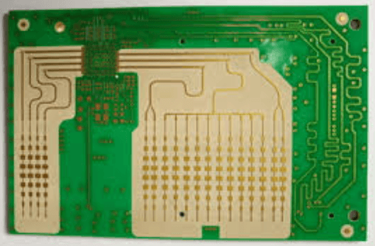
Printed Circuit Board (PCB) prototype development is a critical phase in the design and manufacturing of electronic devices. This stage allows engineers to test and validate their designs before mass production, ensuring functionality and reliability. To achieve this, a variety of essential tools and equipment are required, each playing a pivotal role in the prototyping process. Understanding these tools and their applications is fundamental for anyone involved in PCB development.
Firstly, design software is indispensable in the initial stages of PCB prototyping.
Programs such as Altium Designer, Eagle, and KiCad enable engineers to create detailed schematics and layout designs. These software tools offer a range of features, including component libraries, routing options, and simulation capabilities, which help in visualizing the final product and identifying potential issues early on. Transitioning from design to physical creation, the next essential tool is the PCB plotter or printer. This equipment translates the digital design into a physical format, typically by printing the circuit layout onto a transparent film or directly onto the PCB substrate using specialized inks.
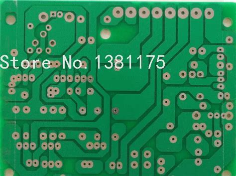
Following the printing process, the PCB must undergo etching to remove unwanted copper and reveal the circuit pathways.
Etching tanks or machines, often using ferric chloride or ammonium persulfate solutions, are employed for this purpose. These chemicals dissolve the excess copper, leaving behind the desired circuit pattern. Safety precautions, such as proper ventilation and protective gear, are crucial when handling these substances to prevent harm.
Once the etching is complete, drilling machines are used to create holes for component leads and vias.
Precision is paramount in this step, as inaccuracies can lead to misalignment and connectivity issues. CNC drilling machines, equipped with fine drill bits, are commonly used to achieve the necessary precision. After drilling, the PCB undergoes a cleaning process to remove any residual chemicals and debris, ensuring a clean surface for component placement.
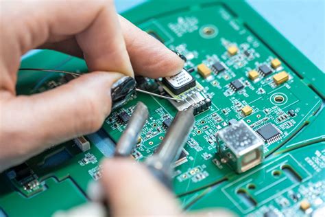
Component placement and soldering are the next critical steps in PCB prototyping.
Pick-and-place machines automate the placement of surface-mount components, significantly increasing efficiency and accuracy. For through-hole components, manual placement is often required. Soldering stations, equipped with temperature-controlled soldering irons and various tips, are essential for securing components to the PCB. Solder paste and reflow ovens are used for surface-mount components, where the paste is applied to the pads, components are placed, and the board is heated to melt the solder, forming secure connections.
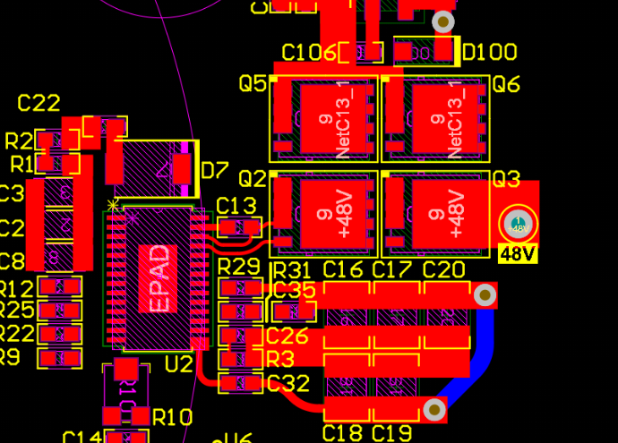
Inspection and testing equipment are vital to ensure the prototype functions as intended.
Optical inspection systems, such as microscopes and automated optical inspection (AOI) machines, help identify soldering defects, misaligned components, and other issues. Electrical testing equipment, including multimeters, oscilloscopes, and logic analyzers, are used to verify circuit functionality and performance. These tools allow engineers to diagnose and rectify any problems before proceeding to the final stages of development.
Finally, environmental testing chambers simulate various conditions, such as temperature and humidity, to assess the prototype’s durability and reliability.
This step is crucial for applications where the PCB will be exposed to harsh environments. By subjecting the prototype to these tests, engineers can ensure that the final product will perform consistently under real-world conditions.
In conclusion, PCB prototype development relies on a comprehensive suite of tools and equipment, each contributing to the accuracy, efficiency, and reliability of the final product. From design software to environmental testing chambers, these tools enable engineers to transform their concepts into functional prototypes, paving the way for successful mass production. Understanding and utilizing these essential tools is fundamental for anyone involved in the intricate process of PCB development.
Top PCB Prototype Equipment For Beginners
Printed Circuit Boards (PCBs) are the backbone of modern electronic devices, and creating prototypes is a crucial step in the development process. For beginners venturing into PCB prototyping, selecting the right equipment can be daunting. However, understanding the essential tools and their functions can significantly ease this journey. This article aims to provide an overview of the top PCB prototype equipment suitable for beginners, ensuring a smooth transition from concept to creation.
To begin with, a reliable PCB design software is indispensable.
Software such as KiCad, Eagle, and Altium Designer are popular choices among novices and professionals alike. These programs offer user-friendly interfaces and comprehensive libraries of components, enabling users to design intricate circuits with ease. Moreover, they provide simulation features that allow for the testing of circuits before physical prototyping, thereby minimizing errors and saving time.
Once the design phase is complete, the next step involves transferring the design onto a physical board.
For this purpose, a laser printer and photoresist materials are essential. The laser printer is used to print the PCB layout onto a transparent sheet, which is then placed over a copper-clad board coated with photoresist. Exposure to UV light hardens the photoresist, creating a mask that protects certain areas of the copper during the etching process. This method is both cost-effective and straightforward, making it ideal for beginners.
Following the exposure process, the board must be developed and etched.
A developer solution, typically a mixture of sodium carbonate and water, is used to remove the unexposed photoresist, revealing the copper underneath. Subsequently, an etching solution, often ferric chloride, is employed to dissolve the exposed copper, leaving behind the desired circuit pattern. It is crucial to handle these chemicals with care, using appropriate safety gear such as gloves and goggles, to prevent any accidents.
After etching, the next step is drilling holes for through-hole components.
A precision drill press is recommended for this task, as it ensures accurate and clean holes. Beginners may find a manual hand drill sufficient for simple projects, but investing in a drill press can significantly improve the quality and precision of the final product. Additionally, carbide drill bits are preferred due to their durability and ability to create smooth holes in the copper-clad board.
Soldering is another critical skill in PCB prototyping. A high-quality soldering iron with adjustable temperature settings is essential for achieving clean and reliable solder joints.
Beginners should also consider using lead-free solder, which is safer and more environmentally friendly. Alongside the soldering iron, a set of tweezers, a desoldering pump, and solder wick are useful tools for handling small components and correcting mistakes.
Finally, a multimeter is an invaluable tool for testing and troubleshooting the completed PCB.
This device measures voltage, current, and resistance, allowing users to verify the functionality of their circuits and identify any issues. For beginners, a digital multimeter with auto-ranging capabilities is recommended, as it simplifies the measurement process and reduces the likelihood of errors.
In conclusion, embarking on PCB prototyping requires a combination of design software, printing and etching materials, drilling equipment, soldering tools, and testing devices. By investing in these essential pieces of equipment, beginners can confidently navigate the complexities of PCB creation and bring their electronic projects to life. With practice and patience, the process will become more intuitive, paving the way for more advanced and intricate designs in the future.
Advanced PCB Prototype Machines For Professionals
In the realm of electronics, the development of printed circuit boards (PCBs) is a critical step that bridges the gap between conceptual design and functional hardware. For professionals in the field, the precision and efficiency of PCB prototype machines are paramount. These advanced machines are designed to meet the rigorous demands of modern electronics, ensuring that prototypes are not only accurate but also produced in a timely manner.
To begin with, the evolution of PCB prototype equipment has been driven by the need for higher precision and faster turnaround times.
Traditional methods, which often involved manual processes and multiple iterations, have given way to automated systems that can produce complex designs with minimal human intervention. This shift has been facilitated by advancements in computer-aided design (CAD) software, which allows for intricate designs to be translated directly into machine-readable formats.
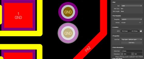
One of the key features of advanced PCB prototype machines is their ability to handle high-density interconnects (HDI).
HDI technology is essential for modern electronics, where space is at a premium and components are densely packed. These machines are equipped with high-resolution laser systems that can create fine traces and vias, ensuring that even the most complex designs can be accurately reproduced. Moreover, the integration of automated optical inspection (AOI) systems ensures that any defects are detected early in the process, reducing the likelihood of costly rework.
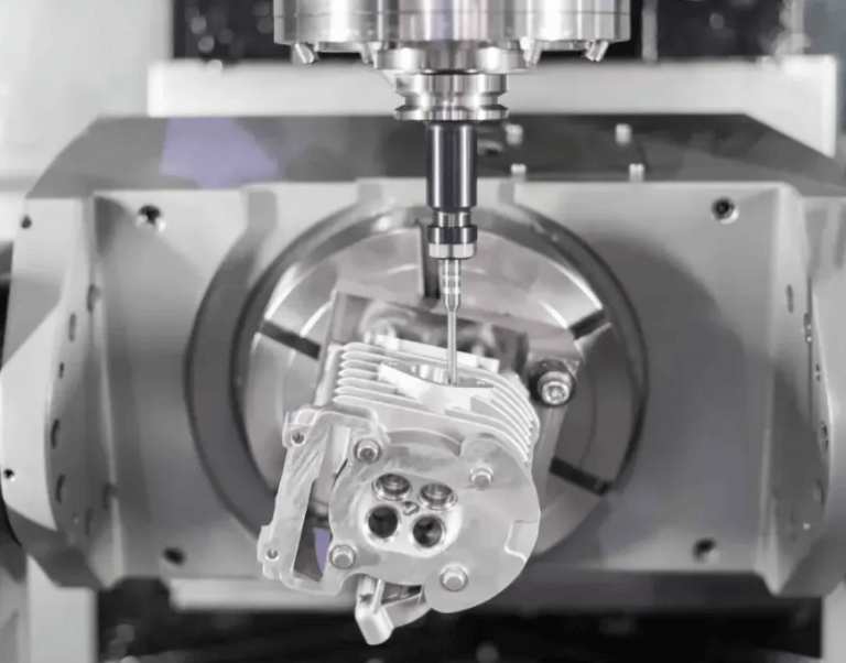
In addition to precision, speed is a critical factor for professionals working with PCB prototypes.
Advanced machines are capable of rapid prototyping, significantly reducing the time from design to physical board. This is particularly important in industries such as aerospace, automotive, and consumer electronics, where time-to-market can be a decisive factor in a product’s success. By leveraging high-speed milling and drilling capabilities, these machines can produce prototypes in a fraction of the time required by traditional methods.
Furthermore, the versatility of modern PCB prototype equipment cannot be overstated.
These machines are designed to work with a wide range of materials, from standard FR4 to advanced substrates like Rogers and polyimide. This flexibility allows professionals to experiment with different materials to achieve the desired electrical and thermal properties for their designs. Additionally, the ability to produce multi-layer boards with precise alignment and registration opens up new possibilities for complex circuit designs.
Another significant advantage of advanced PCB prototype machines is their integration with other manufacturing processes.
For instance, many of these machines are equipped with surface-mount technology (SMT) capabilities, allowing for the direct placement of components onto the board. This seamless integration streamlines the prototyping process, enabling professionals to move from bare board to fully assembled prototype in a single workflow. Consequently, this reduces the potential for errors and accelerates the overall development cycle.
Moreover, the user-friendly interfaces of these machines make them accessible to a broader range of professionals.
While the underlying technology is highly sophisticated, manufacturers have focused on creating intuitive software that simplifies the operation of these machines. This democratization of advanced PCB prototyping technology means that even smaller firms and independent designers can take advantage of these powerful tools.
In conclusion, advanced PCB prototype machines represent a significant leap forward for professionals in the electronics industry. By combining precision, speed, versatility, and integration, these machines enable the rapid development of high-quality prototypes. As technology continues to advance, it is likely that these machines will become even more capable, further pushing the boundaries of what is possible in PCB design and manufacturing.
Cost-Effective PCB Prototype Solutions For Startups
In the rapidly evolving landscape of technology, startups often find themselves at the forefront of innovation, striving to bring groundbreaking products to market.
One critical component in the development of electronic devices is the printed circuit board (PCB).
However, the journey from concept to production can be fraught with challenges, particularly for startups operating on limited budgets. Cost-effective PCB prototype solutions, therefore, become indispensable for these burgeoning enterprises.
To begin with, the importance of PCB prototypes cannot be overstated.
Prototyping allows startups to test and validate their designs before committing to full-scale production. This iterative process helps in identifying and rectifying potential flaws, ensuring that the final product meets the desired specifications and performance standards. However, traditional PCB prototyping methods can be prohibitively expensive, often involving high setup costs and long lead times. This is where cost-effective solutions come into play, offering startups a viable path to innovation without breaking the bank.
One of the most significant advancements in this domain is the advent of desktop PCB prototyping equipment.
These compact, user-friendly machines enable startups to produce high-quality PCB prototypes in-house, drastically reducing both costs and turnaround times. By eliminating the need for outsourcing, startups can maintain greater control over their design process, making real-time adjustments as needed. Moreover, the initial investment in such equipment is often offset by the savings accrued from avoiding external prototyping services.
In addition to desktop prototyping equipment, another cost-effective solution lies in leveraging online PCB manufacturing services.
These platforms offer a range of options tailored to the needs of startups, from single-layer to multi-layer PCBs, with varying degrees of complexity. By utilizing these services, startups can benefit from economies of scale, as these manufacturers often handle large volumes of orders, thereby reducing per-unit costs. Furthermore, many online PCB manufacturers provide design verification tools, ensuring that the submitted designs are manufacturable and free from errors, thus minimizing the risk of costly rework.
Transitioning from traditional methods to these modern solutions also brings about a significant reduction in lead times.
Desktop prototyping equipment allows for rapid iteration, enabling startups to move from design to prototype in a matter of hours. Similarly, online PCB manufacturing services often offer expedited shipping options, ensuring that prototypes are delivered within days rather than weeks. This acceleration in the development cycle is crucial for startups, as it allows them to bring their products to market faster, gaining a competitive edge.
Moreover, the integration of advanced software tools has further streamlined the PCB prototyping process.
Design software with built-in simulation and testing capabilities enables startups to conduct thorough analyses of their circuits before physical prototyping. This not only enhances the accuracy of the prototypes but also reduces the likelihood of errors, thereby saving both time and resources. Additionally, many of these software tools are available through affordable subscription models, making them accessible to startups with limited financial resources.
In conclusion, cost-effective PCB prototype solutions are essential for startups aiming to innovate within the constraints of a tight budget. The combination of desktop prototyping equipment, online manufacturing services, and advanced design software provides a comprehensive toolkit for these enterprises. By adopting these modern approaches, startups can streamline their development processes, reduce costs, and accelerate their time-to-market, ultimately positioning themselves for success in the competitive tech industry.