Pcb prototype pick and place
Understanding The Basics Of PCB Prototype Pick And Place
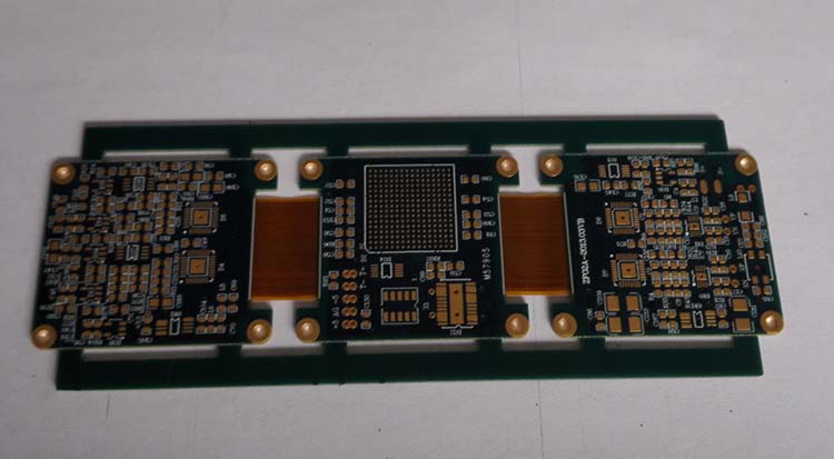
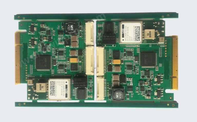
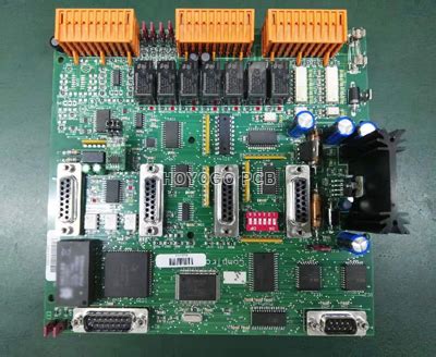
Printed Circuit Board (PCB) prototype pick and place is a critical process in the development and manufacturing of electronic devices. This procedure involves the precise placement of electronic components onto a PCB, which serves as the foundation for electronic circuits. Understanding the basics of this process is essential for anyone involved in electronics design and manufacturing, as it directly impacts the functionality and reliability of the final product.
To begin with, the PCB prototype pick and place process starts with the design of the PCB layout.
Engineers use specialized software to create a detailed schematic of the circuit, specifying the exact locations where each component should be placed. This design phase is crucial, as any errors or misplacements can lead to malfunctioning circuits or even complete failure of the device. Once the design is finalized, it is converted into a format that can be read by pick and place machines.
These machines are sophisticated pieces of equipment that automate the placement of components onto the PCB.
They use a combination of vision systems, precision mechanics, and software algorithms to accurately position each component. The process begins with the machine picking up a component from a feeder, which holds a supply of components in a specific orientation. The machine then moves the component to the correct location on the PCB and places it with high precision. This is repeated for each component until the entire board is populated.
One of the key advantages of using pick and place machines is their speed and accuracy.
Manual placement of components can be time-consuming and prone to human error, especially for complex boards with hundreds or thousands of components. In contrast, pick and place machines can place components at a rate of thousands per hour, with placement accuracy often within a few micrometers. This not only speeds up the manufacturing process but also ensures a higher level of consistency and reliability in the final product.
However, the effectiveness of the pick and place process depends on several factors.
The quality of the components and the PCB itself is paramount. Components must be free of defects and properly packaged to ensure they can be picked up and placed accurately. Similarly, the PCB must be manufactured to precise specifications, with clean and well-defined pads for component placement. Any deviations can lead to placement errors or poor solder joints, which can affect the performance of the circuit.
Another important aspect is the programming and calibration of the pick and place machine.
Operators must ensure that the machine is correctly programmed with the PCB layout and component data. This includes specifying the exact coordinates for each component, as well as any special handling requirements. Regular calibration and maintenance of the machine are also necessary to maintain its accuracy and reliability over time.
In conclusion, PCB prototype pick and place is a vital process in the electronics manufacturing industry. It combines advanced technology and precise engineering to ensure that electronic components are accurately placed on PCBs, leading to reliable and high-performing electronic devices. By understanding the basics of this process, engineers and manufacturers can optimize their workflows, reduce errors, and produce high-quality products that meet the demands of today’s technology-driven world.
Top Challenges In PCB Prototype Pick And Place And How To Overcome Them
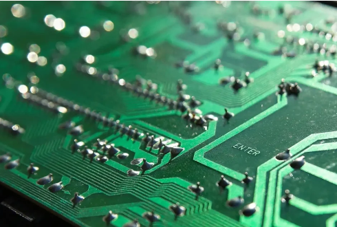
The process of PCB prototype pick and place is a critical phase in the development of electronic devices, involving the precise placement of components onto a printed circuit board (PCB). Despite advancements in technology, several challenges persist in this domain, posing significant hurdles for engineers and manufacturers. Understanding these challenges and implementing effective strategies to overcome them is essential for ensuring the efficiency and reliability of PCB prototypes.
One of the foremost challenges in PCB prototype pick and place is the accurate alignment of components.
Given the miniaturization of electronic components, even the slightest misalignment can lead to functional failures or reduced performance of the final product. To address this issue, it is crucial to employ high-precision pick and place machines equipped with advanced vision systems. These systems utilize cameras and image recognition software to ensure components are placed with pinpoint accuracy. Additionally, regular calibration and maintenance of these machines can further enhance their precision, thereby minimizing alignment errors.
Another significant challenge is the handling of diverse component types and sizes.
Modern PCBs often incorporate a wide variety of components, ranging from tiny surface-mount devices (SMDs) to larger through-hole components. This diversity can complicate the pick and place process, as different components require different handling techniques. To mitigate this challenge, manufacturers can invest in versatile pick and place machines capable of accommodating various component types. Furthermore, the use of specialized nozzles and feeders designed for specific components can improve handling efficiency and reduce the risk of damage during placement.
Component availability and lead times also pose considerable challenges in PCB prototype pick and place.
The rapid pace of technological innovation often results in short product life cycles, leading to frequent changes in component availability. This can disrupt production schedules and delay the development of prototypes. To overcome this challenge, it is advisable to establish strong relationships with multiple suppliers and maintain a well-managed inventory of critical components. Additionally, adopting a flexible design approach that allows for the substitution of equivalent components can help mitigate the impact of supply chain disruptions.
The complexity of PCB designs is another factor that can complicate the pick and place process.
As electronic devices become more sophisticated, PCBs are increasingly populated with densely packed components and intricate routing. This complexity can increase the likelihood of placement errors and make it difficult to achieve consistent quality. To address this issue, engineers should employ design for manufacturability (DFM) principles during the PCB layout phase. By optimizing the design for ease of assembly, such as ensuring adequate spacing between components and minimizing the number of unique component types, the pick and place process can be streamlined and the risk of errors reduced.
Finally, the challenge of ensuring quality control throughout the pick and place process cannot be overlooked.
Even with advanced machinery and meticulous planning, defects can still occur. Implementing robust inspection and testing protocols is essential to identify and rectify any issues early in the production cycle. Automated optical inspection (AOI) systems and in-circuit testing (ICT) are valuable tools that can detect placement errors, soldering defects, and other anomalies. By integrating these quality control measures into the pick and place process, manufacturers can enhance the reliability and performance of their PCB prototypes.
In conclusion, while the PCB prototype pick and place process presents several challenges, a combination of advanced technology, strategic planning, and rigorous quality control can effectively address these issues. By focusing on precision alignment, versatile handling, component availability, design complexity, and quality assurance, manufacturers can overcome the obstacles and achieve successful PCB prototype development.
Innovations In PCB Prototype Pick And Place Technology
The field of printed circuit board (PCB) manufacturing has witnessed significant advancements over the years, particularly in the realm of PCB prototype pick and place technology. This technology, which involves the precise placement of electronic components onto a PCB, is crucial for the development and testing of new electronic designs. As the demand for more complex and miniaturized electronic devices grows, innovations in PCB prototype pick and place technology have become essential to meet these evolving requirements.
One of the most notable innovations in this area is the development of high-speed pick and place machines.
These machines are designed to handle a large number of components with remarkable accuracy and speed. By utilizing advanced vision systems and sophisticated algorithms, modern pick and place machines can identify and place components with micron-level precision. This level of accuracy is particularly important for prototypes, where even the smallest misalignment can lead to significant performance issues or complete failure of the device.
In addition to speed and accuracy, flexibility is another critical aspect of modern pick and place technology.
Traditional pick and place machines were often limited to handling specific types of components or required extensive reconfiguration to accommodate different designs. However, recent innovations have led to the development of highly adaptable machines that can easily switch between different component types and sizes. This flexibility is achieved through the use of modular heads and feeders, which can be quickly swapped out to match the requirements of a particular prototype. Consequently, this reduces downtime and increases the efficiency of the prototyping process.
Moreover, the integration of artificial intelligence (AI) and machine learning (ML) into pick and place technology has further enhanced its capabilities.
AI-driven systems can analyze vast amounts of data from previous placements to optimize the placement process for future prototypes. By learning from past errors and successes, these systems can predict potential issues and adjust their operations accordingly. This predictive capability not only improves the accuracy and reliability of component placement but also reduces the likelihood of costly rework or redesigns.
Another significant innovation is the incorporation of real-time monitoring and feedback systems.
These systems provide continuous oversight of the pick and place process, allowing for immediate detection and correction of any anomalies. For instance, if a component is not placed correctly, the system can halt the process, alert the operator, and provide detailed information on the issue. This real-time feedback loop ensures that any problems are addressed promptly, thereby maintaining the integrity of the prototype.
Furthermore, advancements in software have played a crucial role in enhancing PCB prototype pick and place technology.
Modern software solutions offer comprehensive design and simulation tools that enable engineers to create detailed placement plans before actual production begins. These tools can simulate the entire pick and place process, identifying potential challenges and optimizing the layout for maximum efficiency. By addressing issues in the virtual environment, engineers can save time and resources during the physical prototyping stage.
In conclusion, the innovations in PCB prototype pick and place technology have significantly improved the speed, accuracy, flexibility, and reliability of the prototyping process. High-speed machines, adaptable systems, AI and ML integration, real-time monitoring, and advanced software solutions have collectively transformed the landscape of PCB manufacturing. As electronic devices continue to evolve, these technological advancements will play a pivotal role in enabling the development of increasingly sophisticated and miniaturized prototypes, ultimately driving progress in the electronics industry.
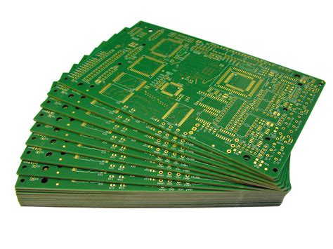
Step-By-Step Guide To Setting Up A PCB Prototype Pick And Place Machine
Setting up a PCB prototype pick and place machine is a meticulous process that requires careful attention to detail and a methodical approach. The first step in this process involves preparing the workspace. It is essential to ensure that the environment is clean and free from dust, as contaminants can adversely affect the performance of the machine and the quality of the PCB prototypes. Additionally, the workspace should be well-lit and organized, with all necessary tools and materials readily accessible.
Once the workspace is prepared, the next step is to unbox and inspect the pick and place machine.
Carefully remove the machine from its packaging, taking care to avoid any damage. Inspect the machine for any signs of damage that may have occurred during shipping. If any issues are found, it is crucial to contact the manufacturer immediately. Assuming the machine is in good condition, proceed to set it up according to the manufacturer’s instructions. This typically involves attaching various components, such as the feeder units and the placement head, and connecting the machine to a power source.
Following the physical setup, the next phase involves installing the necessary software.
Most pick and place machines come with proprietary software that must be installed on a computer. This software is used to control the machine and program the placement of components on the PCB. Install the software according to the manufacturer’s instructions, and ensure that it is compatible with your operating system. Once installed, launch the software and familiarize yourself with its interface and features.
With the software installed, the next step is to load the PCB design files into the software.
These files, typically in Gerber format, contain the layout and placement information for the components on the PCB. Import the files into the software and verify that the design is correctly displayed. It is also important to check for any errors or discrepancies in the design that could affect the placement process.
After verifying the design, the next step is to set up the feeders.
Feeders are used to hold and dispense the components that will be placed on the PCB. Load the components into the appropriate feeders, ensuring that each component is correctly oriented and securely held in place. The software will typically provide a feeder setup guide, which indicates the correct feeder positions for each component. Follow this guide carefully to ensure accurate placement.
Once the feeders are set up, the next step is to calibrate the machine.
Calibration ensures that the machine accurately picks up and places components on the PCB. This process typically involves using a calibration tool or jig to align the placement head and verify its accuracy. Follow the manufacturer’s instructions for calibration, and make any necessary adjustments to ensure optimal performance.
With the machine calibrated, the final step is to run a test placement.
Load a blank PCB into the machine and run a test program to verify that the machine is correctly placing components. Inspect the test PCB for any placement errors or misalignments, and make any necessary adjustments to the machine or software settings. Once you are satisfied with the test results, the machine is ready for production.
In conclusion, setting up a PCB prototype pick and place machine involves several detailed steps, from preparing the workspace to running a test placement. By following these steps carefully and methodically, you can ensure that your machine is set up correctly and ready to produce high-quality PCB prototypes.