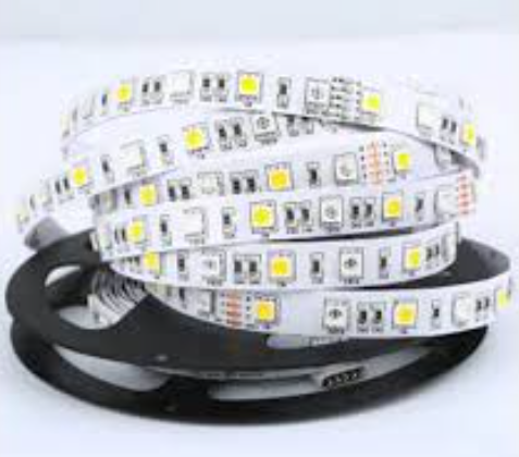
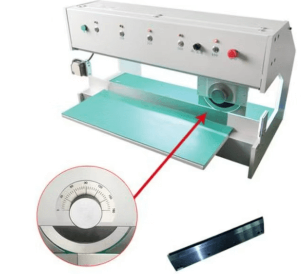
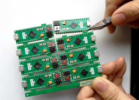
Pcb rails
Importance Of PCB Rails In Circuit Design
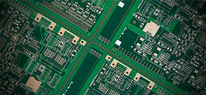
Printed Circuit Boards (PCBs) are the backbone of modern electronic devices, providing the necessary platform for mounting and interconnecting various electronic components.
Among the many elements that contribute to the functionality and reliability of PCBs, PCB rails hold a significant place. These rails, often overlooked, play a crucial role in ensuring the structural integrity and electrical performance of the circuit design.
To begin with, PCB rails are essential for maintaining the mechanical stability of the board.
They provide a rigid framework that supports the entire PCB, preventing it from bending or warping during manufacturing, assembly, and operation. This structural support is particularly important in applications where the PCB is subjected to mechanical stress, such as in automotive or industrial environments. By maintaining the flatness and rigidity of the board, PCB rails help to ensure that the components remain securely attached and that the electrical connections are not compromised.
In addition to mechanical stability, PCB rails also contribute to the thermal management of the circuit.
Electronic components generate heat during operation, and effective heat dissipation is critical to prevent overheating and ensure reliable performance. PCB rails can act as heat sinks, conducting heat away from the components and distributing it more evenly across the board. This helps to maintain optimal operating temperatures and prolong the lifespan of the components. Furthermore, by providing a pathway for heat to escape, PCB rails can reduce the need for additional cooling solutions, such as fans or heat sinks, thereby simplifying the overall design and reducing costs.
Another important aspect of PCB rails is their role in facilitating the manufacturing process.
During the assembly of PCBs, the boards are often handled by automated machinery that requires precise alignment and positioning. PCB rails provide reference points and alignment features that ensure the accurate placement of components and the proper registration of solder masks and other layers. This precision is crucial for achieving high-quality solder joints and reliable electrical connections. Moreover, PCB rails can also serve as attachment points for fixtures and tooling used during the assembly process, further enhancing the efficiency and accuracy of manufacturing.
From an electrical perspective, PCB rails can also serve as ground planes or power distribution networks.
Ground planes are essential for providing a low-impedance path for return currents, reducing electromagnetic interference (EMI) and improving signal integrity. By incorporating PCB rails as ground planes, designers can achieve better noise performance and more stable operation of the circuit. Similarly, PCB rails can be used to distribute power to various components, ensuring that each part of the circuit receives a stable and consistent supply voltage. This is particularly important in complex designs with multiple power domains or high-current requirements.
In conclusion, PCB rails are a vital component of circuit design, offering numerous benefits that enhance the mechanical, thermal, and electrical performance of the board.
By providing structural support, aiding in thermal management, facilitating manufacturing, and serving as ground planes or power distribution networks, PCB rails contribute to the overall reliability and functionality of electronic devices. As technology continues to advance and the demand for more compact and efficient designs grows, the importance of PCB rails in circuit design will only become more pronounced. Therefore, it is essential for designers to carefully consider the incorporation of PCB rails in their designs to ensure optimal performance and longevity of their electronic products.
How To Optimize PCB Rail Layout For Signal Integrity
Optimizing the layout of PCB rails is crucial for maintaining signal integrity in electronic designs. Signal integrity refers to the quality and reliability of electrical signals as they travel through a printed circuit board (PCB). Poor signal integrity can lead to data corruption, increased error rates, and overall system instability. Therefore, understanding how to optimize PCB rail layout is essential for engineers and designers aiming to create robust and efficient electronic systems.
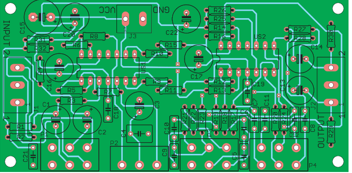
To begin with, it is important to consider the placement of power and ground rails.
These rails serve as the backbone of the PCB, providing the necessary power and reference points for all components. Ensuring that power and ground rails are properly placed can significantly reduce noise and improve signal integrity. One effective strategy is to use a ground plane, which is a continuous layer of copper that serves as a common reference point for all signals. A ground plane can help to minimize electromagnetic interference (EMI) and provide a low-impedance path for return currents.
In addition to the placement of power and ground rails, the routing of signal traces is another critical factor in optimizing PCB rail layout.
Signal traces should be kept as short and direct as possible to minimize the potential for signal degradation. When routing high-speed signals, it is important to avoid sharp bends and to use controlled impedance traces. Controlled impedance traces are designed to have a specific impedance, which helps to maintain signal integrity by reducing reflections and signal loss.
Another important consideration is the separation of different types of signals.
High-speed digital signals, analog signals, and power signals should be routed separately to prevent crosstalk and interference. Crosstalk occurs when a signal in one trace induces an unwanted signal in an adjacent trace, which can lead to data corruption and signal degradation. By maintaining adequate spacing between different types of signals, designers can reduce the risk of crosstalk and improve overall signal integrity.
Furthermore, the use of decoupling capacitors can play a significant role in optimizing PCB rail layout.
Decoupling capacitors are used to filter out noise and provide a stable power supply to components. Placing decoupling capacitors close to the power pins of integrated circuits (ICs) can help to reduce voltage fluctuations and improve signal integrity. It is also important to use capacitors with appropriate values and to place them strategically throughout the PCB to ensure effective noise suppression.
Thermal management is another aspect that should not be overlooked when optimizing PCB rail layout.
Excessive heat can affect the performance and reliability of electronic components, leading to signal degradation and potential failure. Proper thermal management techniques, such as the use of thermal vias and heat sinks, can help to dissipate heat and maintain signal integrity. Thermal vias are small holes filled with conductive material that provide a path for heat to escape from the PCB, while heat sinks are used to absorb and dissipate heat from high-power components.
In conclusion, optimizing PCB rail layout for signal integrity involves careful consideration of various factors, including the placement of power and ground rails, the routing of signal traces, the separation of different types of signals, the use of decoupling capacitors, and effective thermal management. By paying attention to these details, designers can create PCBs that deliver reliable and high-quality performance, ensuring the success of their electronic systems.
Common Mistakes To Avoid When Designing PCB Rails
When designing PCB rails, it is crucial to avoid common mistakes that can compromise the functionality and reliability of the final product. One of the most frequent errors is neglecting proper power distribution. Ensuring that power is evenly distributed across the PCB is essential to prevent voltage drops and power losses. This can be achieved by using wider traces for power rails and placing decoupling capacitors close to the power pins of integrated circuits. Additionally, it is important to consider the current-carrying capacity of the traces. Undersized traces can lead to overheating and potential failure of the PCB.
Another common mistake is poor grounding practices.
A solid ground plane is vital for reducing noise and ensuring signal integrity. Designers should avoid creating ground loops, which can introduce unwanted noise and interfere with the performance of the PCB. Instead, a single, continuous ground plane should be used, and all ground connections should be made to this plane. Furthermore, it is advisable to place ground vias strategically to minimize the impedance of the ground path.
Thermal management is another critical aspect that is often overlooked.
Components that generate significant heat need to be adequately cooled to maintain their performance and longevity. This can be achieved by incorporating thermal vias, heat sinks, and proper component placement to facilitate heat dissipation. Failing to address thermal issues can lead to overheating, which can cause components to fail or degrade over time.
Signal integrity is another area where designers frequently make mistakes.
High-speed signals require careful routing to avoid issues such as crosstalk, signal reflection, and electromagnetic interference. To mitigate these problems, designers should use controlled impedance traces, maintain consistent trace widths, and avoid sharp bends. Additionally, differential pairs should be routed together with equal lengths to ensure signal integrity.
Component placement is another critical factor in PCB design.
Placing components too close together can lead to difficulties in assembly and potential short circuits. It is essential to follow the manufacturer’s recommended spacing guidelines and consider the ease of soldering and inspection. Moreover, placing components in a logical and organized manner can simplify troubleshooting and repair processes.
Designers should also be mindful of the PCB layout software they use.
While these tools offer numerous features to aid in the design process, relying too heavily on automated functions can lead to suboptimal results. It is important to manually review and adjust the layout to ensure that all design rules and best practices are followed.
Lastly, thorough testing and validation are crucial steps that should not be overlooked.
Prototyping and testing the PCB design can help identify and rectify any issues before mass production. This includes performing electrical tests, thermal analysis, and signal integrity assessments. By thoroughly validating the design, designers can ensure that the final product meets all performance and reliability requirements.
In conclusion, avoiding common mistakes in PCB rail design requires careful attention to power distribution, grounding practices, thermal management, signal integrity, component placement, and thorough testing. By adhering to these best practices, designers can create reliable and efficient PCBs that meet the demands of modern electronic applications.
Advanced Techniques For Managing Power Distribution With PCB Rails
Printed Circuit Boards (PCBs) are the backbone of modern electronic devices, providing the necessary infrastructure for electrical connections and component support. Among the various techniques employed to enhance the functionality and reliability of PCBs, managing power distribution effectively is paramount. One advanced method for achieving this is through the use of PCB rails. These rails, essentially conductive pathways, play a crucial role in ensuring that power is distributed efficiently and consistently across the board.
To begin with, PCB rails are designed to handle the power requirements of different components on the board.
By providing a dedicated path for power distribution, they help in minimizing voltage drops and power losses, which are common issues in complex circuits. This is particularly important in high-frequency applications where even minor fluctuations in power can lead to significant performance degradation. Moreover, PCB rails can be tailored to meet the specific needs of the circuit, allowing for greater flexibility in design and implementation.
In addition to their primary function of power distribution, PCB rails also contribute to the overall thermal management of the board.
As electronic components operate, they generate heat, which needs to be dissipated to maintain optimal performance and prevent damage. PCB rails, being made of conductive materials such as copper, can act as heat sinks, drawing heat away from critical components and distributing it more evenly across the board. This not only enhances the longevity of the components but also improves the overall reliability of the device.
Furthermore, the use of PCB rails can significantly reduce electromagnetic interference (EMI).
EMI is a common issue in electronic circuits, where unwanted electromagnetic waves can disrupt the normal operation of the components. By providing a well-defined path for power distribution, PCB rails help in minimizing the loop areas that are susceptible to EMI. This is particularly beneficial in high-speed digital circuits, where maintaining signal integrity is crucial. Additionally, PCB rails can be designed with specific geometries and placements to further mitigate EMI, ensuring that the circuit operates smoothly and efficiently.
Another advantage of using PCB rails is the simplification of the layout process.
In traditional PCB designs, power distribution often requires multiple layers and complex routing to ensure that all components receive the necessary power. This can lead to increased design time and potential errors. However, with PCB rails, the power distribution network can be more straightforward and easier to implement. This not only speeds up the design process but also reduces the likelihood of errors, leading to a more reliable final product.
Moreover, PCB rails can be integrated with other advanced techniques to further enhance power distribution.
For instance, incorporating decoupling capacitors along the rails can help in stabilizing the power supply and reducing noise. Similarly, using thicker rails or multiple parallel rails can increase the current-carrying capacity, making it suitable for high-power applications. These techniques, when combined with PCB rails, provide a robust solution for managing power distribution in complex electronic circuits.
In conclusion, PCB rails offer a multitude of benefits for managing power distribution in electronic circuits. From minimizing voltage drops and power losses to enhancing thermal management and reducing EMI, they play a critical role in ensuring the reliability and performance of modern electronic devices. By simplifying the layout process and allowing for greater design flexibility, PCB rails represent an advanced technique that can significantly improve the efficiency and effectiveness of power distribution in PCBs.