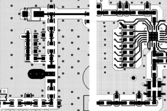
PCB Routing: Best Practices and Techniques for Optimal Design
Introduction
Printed Circuit Board (PCB) routing is a critical step in the design and manufacturing of electronic circuits. It involves connecting various components through conductive traces on the PCB to ensure proper electrical functionality. Effective routing impacts signal integrity, power distribution, electromagnetic compatibility (EMC), and thermal management. Poor routing can lead to signal degradation, crosstalk, power delivery issues, and even complete circuit failure.
This article explores the fundamentals of PCB routing, best practices, and advanced techniques to optimize performance, reliability, and manufacturability.
1. Fundamentals of PCB Routing
1.1 What is PCB Routing?
PCB routing refers to the process of laying out electrical connections (traces) between components on a PCB. It follows the schematic design, where logical connections are defined, and translates them into physical pathways.
1.2 Types of PCB Routing
- Manual Routing: The designer manually places traces, offering full control but requiring expertise.
- Auto-Routing: Software tools automatically route traces based on design rules, saving time but sometimes requiring manual adjustments.
- Interactive Routing: A hybrid approach where the designer guides the auto-router for critical paths.
1.3 Key Considerations in PCB Routing
- Signal Integrity (SI): Ensuring signals travel without distortion.
- Power Integrity (PI): Stable voltage distribution across the board.
- Electromagnetic Compatibility (EMC): Minimizing interference.
- Thermal Management: Preventing overheating.
- Manufacturability: Ensuring the design can be fabricated efficiently.
2. PCB Routing Best Practices
2.1 Planning the Layout
Before routing, a well-organized component placement is essential:
- Group related components (e.g., power supply, analog, digital sections).
- Minimize trace lengths to reduce resistance and inductance.
- Consider signal flow to avoid unnecessary crossings.
2.2 Trace Width and Spacing
- Current Carrying Capacity: Wider traces handle higher currents (use online calculators for width vs. current).
- Impedance Control: High-speed signals require controlled impedance traces (e.g., microstrip or stripline).
- Clearance Rules: Maintain proper spacing to avoid short circuits (IPC standards provide guidelines).
2.3 Layer Stackup Strategy
- Single-Layer PCBs: Simple designs, but limited routing space.
- Double-Layer PCBs: More flexibility, with traces on both sides.
- Multi-Layer PCBs (4+ layers): Essential for complex designs:
- Dedicated power and ground planes reduce noise.
- Signal layers can be shielded between planes.
2.4 Grounding Techniques
- Star Grounding: All ground connections meet at a single point (good for analog circuits).
- Ground Plane: A continuous copper layer provides low-impedance return paths.
- Split Ground Planes: Used to isolate analog and digital grounds, but must be connected at a single point.
2.5 Routing High-Speed Signals
- Minimize Length Mismatches: Ensure matched trace lengths for differential pairs (e.g., USB, HDMI).
- Avoid Sharp Angles: Use 45° or curved traces to prevent impedance discontinuities.
- Via Optimization: Minimize via count in high-speed paths to reduce inductance.
2.6 Power Distribution Network (PDN) Design
- Use Decoupling Capacitors: Place them close to IC power pins to suppress noise.
- Wide Power Traces: Reduce voltage drops in high-current paths.
- Power Planes: Provide stable voltage distribution in multi-layer boards.
2.7 Avoiding Crosstalk and EMI
- Increase Spacing: Keep high-speed traces away from sensitive signals.
- Shielding: Use ground traces or planes between noisy and sensitive signals.
- Differential Signaling: Reduces EMI in high-speed interfaces (e.g., LVDS, PCIe).

3. Advanced PCB Routing Techniques
3.1 Length Matching and Timing Constraints
- Differential Pair Routing: Ensure equal trace lengths to maintain signal synchronization.
- Serpentine Traces: Used to add delay where needed (e.g., DDR memory routing).
3.2 Via Optimization
- Via-in-Pad: Used in high-density designs (e.g., BGA routing).
- Blind and Buried Vias: Reduce layer transitions in complex boards.
- Via Stitching: Multiple vias connect ground planes to reduce inductance.
3.3 RF and Microwave Routing
- Controlled Impedance: Critical for RF signals (50Ω or 75Ω traces).
- Avoid Stubs: Prevent signal reflections in transmission lines.
- Use Grounded Coplanar Waveguides: Improves signal isolation.
3.4 Thermal Management in Routing
- Thermal Vias: Dissipate heat from high-power components.
- Wide Power Traces: Help in heat distribution.
- Copper Pours: Increase heat dissipation in critical areas.
3.5 Design for Manufacturing (DFM) Considerations
- Avoid Acid Traps: Sharp angles in traces can trap etching chemicals.
- Minimum Annular Ring: Ensures vias are properly fabricated.
- Testability: Include test points for debugging and production testing.

4. Common PCB Routing Mistakes and How to Avoid Them
4.1 Ignoring Design Rules
- Solution: Set up design rule checks (DRC) in CAD tools before routing.
4.2 Poor Power Delivery
- Solution: Use adequate power plane layers and decoupling capacitors.
4.3 Excessive Via Usage
- Solution: Optimize layer transitions and use via-in-pad where necessary.
4.4 Neglecting Signal Return Paths
- Solution: Ensure uninterrupted ground planes under high-speed signals.
4.5 Overlooking Thermal Issues
- Solution: Use thermal vias and copper pours for heat dissipation.

5. Tools for PCB Routing
Modern PCB design software includes advanced routing features:
- Altium Designer: Advanced auto-routing and interactive routing.
- Cadence Allegro: High-speed routing with constraint management.
- KiCad: Open-source with decent routing capabilities.
- Eagle (Autodesk): Popular for hobbyists and small projects.
6. Conclusion
PCB routing is a complex yet essential aspect of circuit design. By following best practices—such as proper layer stackup, controlled impedance routing, effective grounding, and thermal management—designers can ensure reliable and high-performance PCBs. Advanced techniques like length matching, via optimization, and RF routing further enhance signal integrity and manufacturability.
Whether designing simple single-layer boards or complex multi-layer systems, understanding PCB routing principles helps avoid common pitfalls and leads to successful electronic products. Continuous learning and leveraging modern CAD tools will further improve routing efficiency and design quality.
By applying these guidelines, engineers can achieve optimal PCB routing for their projects, ensuring functionality, reliability, and manufacturability.


