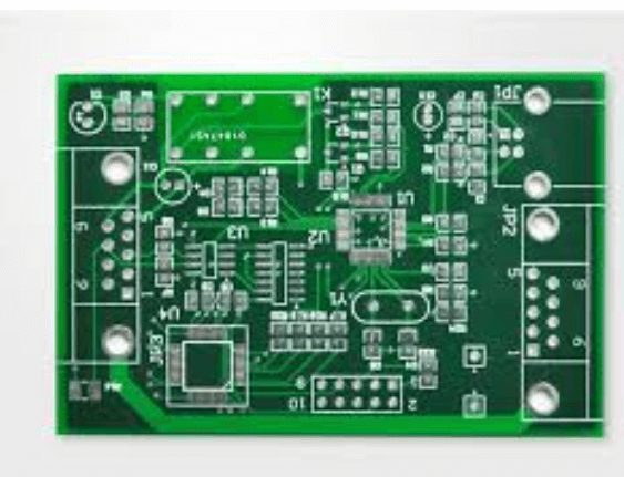
Pcb sample board
Designing Your First PCB Sample Board: A Step-by-Step Guide
Designing your first PCB sample board can be an exciting yet challenging endeavor. The process involves several critical steps, each requiring careful attention to detail to ensure the final product meets your specifications.
To begin with, it is essential to have a clear understanding of the requirements and constraints of your project.
This includes defining the functionality of the PCB, the components to be used, and the physical dimensions of the board. By establishing these parameters early on, you can streamline the design process and avoid potential pitfalls.
Once you have a clear vision of your project, the next step is to create a schematic diagram.
This diagram serves as a blueprint for your PCB, illustrating how the various components will be connected. Using schematic capture software, you can draw the circuit and place the components in their respective positions. It is crucial to double-check the connections and ensure that all components are correctly placed, as any errors at this stage can lead to significant issues later on.
After completing the schematic, the next phase involves designing the PCB layout.
This step translates the schematic diagram into a physical representation of the board. PCB design software can assist in this process by allowing you to place components on the board and route the electrical connections between them. During this stage, it is important to consider factors such as signal integrity, power distribution, and thermal management. Proper placement of components and routing of traces can help minimize noise and interference, ensuring the board functions as intended.
Transitioning from the design phase to the manufacturing phase requires generating the necessary files for production.
These files, commonly known as Gerber files, contain detailed information about the PCB layout, including the copper layers, solder mask, and silkscreen. Additionally, a Bill of Materials (BOM) should be created, listing all the components required for assembly. Ensuring the accuracy of these files is paramount, as any discrepancies can lead to manufacturing errors and delays.
With the Gerber files and BOM in hand, you can proceed to select a PCB manufacturer.
It is advisable to research and choose a reputable manufacturer with experience in producing high-quality PCBs. Communicating your requirements clearly and providing all necessary documentation can help ensure a smooth manufacturing process. Once the boards are produced, they should be thoroughly inspected for any defects or inconsistencies.
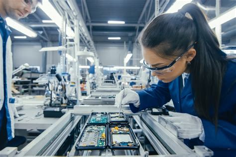
The final step in designing your first PCB sample board is assembly and testing.
Assembling the board involves soldering the components onto the PCB, either manually or using automated equipment. After assembly, the board should undergo rigorous testing to verify its functionality. This may include electrical testing, functional testing, and environmental testing, depending on the specific requirements of your project. Identifying and addressing any issues at this stage is crucial to ensure the final product meets your expectations.
In conclusion, designing your first PCB sample board is a multifaceted process that requires careful planning, attention to detail, and a methodical approach.
By following these steps and utilizing the appropriate tools and resources, you can successfully create a PCB that meets your project’s requirements. While challenges may arise, perseverance and a commitment to quality can lead to a successful outcome, paving the way for future PCB design endeavors.
Top 5 Mistakes to Avoid When Creating PCB Sample Boards
Creating PCB sample boards is a critical step in the development of electronic devices, as it allows engineers to test and validate their designs before moving to mass production. However, this process is fraught with potential pitfalls that can lead to costly delays and suboptimal performance. To ensure the success of your PCB sample boards, it is essential to be aware of and avoid common mistakes.
One of the most frequent errors is inadequate planning and design.
Before even beginning the physical creation of a PCB sample board, it is crucial to have a comprehensive design plan. This includes detailed schematics, a clear understanding of the electrical requirements, and a well-thought-out layout. Neglecting this step can result in design flaws that are difficult and expensive to rectify later.
Another common mistake is the improper selection of materials.
The choice of substrate, copper thickness, and other materials can significantly impact the performance and durability of the PCB. For instance, using a substrate that cannot withstand the operating temperature of the device can lead to premature failure. Therefore, it is essential to select materials that meet the specific requirements of your application. Additionally, it is important to consider the compatibility of these materials with the manufacturing processes you intend to use.
Transitioning to the manufacturing stage, errors in component placement and soldering are also prevalent.
Misplaced components can lead to short circuits, signal integrity issues, and other functional problems. To avoid this, it is advisable to use automated placement machines and to double-check the placement before soldering. Furthermore, improper soldering techniques can result in weak joints that may fail under stress. Ensuring that the soldering process is carried out under controlled conditions and using the appropriate soldering materials can mitigate these risks.
Moreover, inadequate testing and validation of the PCB sample board can lead to undetected issues that manifest during later stages of development or even after deployment.
Comprehensive testing should include electrical testing, thermal testing, and mechanical testing to ensure that the board meets all performance criteria. Skipping or rushing through this phase can result in overlooking critical flaws that could compromise the functionality and reliability of the final product.
Lastly, poor documentation and communication can also hinder the successful creation of PCB sample boards.
Clear and detailed documentation of the design, materials, and manufacturing processes is essential for ensuring that all team members are on the same page. This documentation should be updated regularly to reflect any changes or modifications made during the development process. Effective communication among team members, as well as with external suppliers and manufacturers, is also crucial for avoiding misunderstandings and ensuring that the project stays on track.
In conclusion, creating PCB sample boards is a complex process that requires careful planning, material selection, precise manufacturing, thorough testing, and effective communication. By being aware of and avoiding these common mistakes, you can enhance the quality and reliability of your PCB sample boards, ultimately leading to more successful electronic products.
Innovative Techniques for Testing PCB Sample Boards
Printed Circuit Boards (PCBs) are the backbone of modern electronic devices, and their reliability is paramount. To ensure the highest quality, innovative techniques for testing PCB sample boards have been developed, each offering unique advantages. These methods are essential for identifying potential issues early in the production process, thereby saving time and resources.
One of the most widely used techniques is Automated Optical Inspection (AOI).
AOI employs high-resolution cameras to capture detailed images of the PCB sample board. These images are then compared to a predefined template to identify discrepancies such as missing components, soldering defects, or misalignments. The precision of AOI allows for the rapid detection of even the smallest flaws, making it an invaluable tool in the quality assurance process. Furthermore, AOI systems can be integrated into the production line, providing real-time feedback and enabling immediate corrective actions.
In addition to AOI, X-ray inspection is another critical technique for testing PCB sample boards.
This method is particularly useful for examining the internal structures of the board, such as solder joints and hidden connections. By using X-rays, inspectors can detect voids, cracks, and other internal defects that are not visible to the naked eye. This non-destructive testing method ensures that the integrity of the PCB is maintained while providing a comprehensive analysis of its internal features. Consequently, X-ray inspection is often employed in the final stages of production to verify the overall quality of the board.
Another innovative technique is In-Circuit Testing (ICT), which involves the use of a bed-of-nails tester to make electrical contact with various points on the PCB.
ICT allows for the measurement of electrical parameters such as resistance, capacitance, and inductance, ensuring that each component is functioning correctly. This method is highly effective for detecting issues such as short circuits, open circuits, and incorrect component values. Moreover, ICT can be automated, making it suitable for high-volume production environments where speed and accuracy are crucial.
Complementing ICT is Functional Testing, which evaluates the PCB sample board’s performance under real-world conditions.
This technique involves simulating the board’s operational environment and verifying that it performs as expected. Functional Testing is particularly important for complex PCBs with multiple interconnected components, as it ensures that the entire system operates cohesively. By identifying functional issues early, manufacturers can make necessary adjustments before the board is integrated into the final product.
Additionally, Boundary Scan Testing, also known as JTAG testing, is a powerful method for testing PCB sample boards.
This technique leverages the IEEE 1149.1 standard to test the interconnections between integrated circuits without requiring physical access to the board. Boundary Scan Testing is highly effective for detecting faults in densely populated PCBs where traditional testing methods may be impractical. It also allows for the testing of individual components and their interconnections, providing a thorough assessment of the board’s overall functionality.
Finally, Environmental Stress Screening (ESS) is a technique used to expose PCB sample boards to extreme conditions such as temperature variations, humidity, and vibration. ESS aims to identify latent defects that may not be apparent under normal operating conditions but could lead to failures in the field. By subjecting the boards to these stressors, manufacturers can ensure that only the most robust and reliable PCBs make it to market.
In conclusion, the testing of PCB sample boards is a critical step in the manufacturing process, and the use of innovative techniques such as AOI, X-ray inspection, ICT, Functional Testing, Boundary Scan Testing, and ESS ensures the highest quality and reliability. These methods not only help in identifying potential issues early but also contribute to the overall efficiency and success of the production process.
The Future of PCB Sample Boards: Trends and Predictions
The future of PCB sample boards is poised for significant transformation, driven by advancements in technology and evolving industry demands. As the backbone of modern electronics, printed circuit boards (PCBs) are integral to the functionality of a wide array of devices, from consumer electronics to sophisticated industrial machinery. Consequently, the development and refinement of PCB sample boards are critical to ensuring the reliability and performance of these devices. Several emerging trends and predictions are shaping the future landscape of PCB sample boards, promising to enhance their capabilities and applications.
One of the most notable trends is the increasing miniaturization of electronic components.
As devices become smaller and more compact, the need for PCB sample boards that can accommodate these diminutive components becomes paramount. This trend is driving innovations in PCB design and manufacturing processes, enabling the creation of boards with higher component densities and finer traces. Advanced fabrication techniques, such as laser direct imaging and precision drilling, are being employed to achieve the necessary precision and accuracy. Additionally, the use of high-density interconnect (HDI) technology is becoming more prevalent, allowing for the integration of more components in a smaller footprint.
Another significant trend is the growing adoption of flexible and rigid-flex PCBs.
These boards offer greater design versatility and can be used in applications where traditional rigid PCBs are not feasible. Flexible PCBs are particularly advantageous in wearable technology, medical devices, and other applications where space constraints and mechanical flexibility are critical. The development of new materials and manufacturing techniques is further enhancing the performance and reliability of flexible and rigid-flex PCBs, making them an increasingly attractive option for a wide range of applications.
The rise of the Internet of Things (IoT) is also having a profound impact on the future of PCB sample boards.
IoT devices require PCBs that are not only compact but also capable of supporting wireless communication and low-power operation. This has led to the development of PCBs with integrated antennas and advanced power management features. Moreover, the need for rapid prototyping and iterative design in IoT development is driving the demand for PCB sample boards that can be quickly and easily produced. Additive manufacturing, or 3D printing, is emerging as a promising solution in this regard, enabling the rapid production of custom PCB prototypes with complex geometries.
Sustainability is another key consideration shaping the future of PCB sample boards.
As environmental concerns become more pressing, there is a growing emphasis on developing eco-friendly PCB materials and manufacturing processes. This includes the use of lead-free solder, biodegradable substrates, and energy-efficient production methods. Additionally, efforts are being made to improve the recyclability of PCBs, reducing electronic waste and minimizing the environmental impact of discarded electronics.
In conclusion, the future of PCB sample boards is being shaped by a confluence of technological advancements and industry trends. Miniaturization, flexible and rigid-flex designs, IoT integration, and sustainability are all driving innovations in PCB design and manufacturing. As these trends continue to evolve, PCB sample boards will become increasingly sophisticated, enabling the development of more advanced and reliable electronic devices. The ongoing advancements in this field promise to unlock new possibilities and applications, ensuring that PCB sample boards remain at the forefront of electronic innovation.


