PCB Shielding Techniques: Ensuring Signal Integrity and Electromagnetic Compatibility
Introduction
Printed Circuit Boards (PCBs) are the backbone of modern electronics, serving as the foundation for the interconnection and support of various electronic components. As electronic devices become more complex and operate at higher frequencies, the need for effective PCB shielding techniques has become increasingly critical. Shielding is essential to ensure signal integrity, prevent electromagnetic interference (EMI), and maintain electromagnetic compatibility (EMC). This article explores various PCB shielding techniques, their importance, and their implementation in modern electronic design.
1. Understanding the Need for PCB Shielding
1.1 Electromagnetic Interference (EMI)
EMI is a disturbance generated by an external source that affects the performance of an electrical circuit. It can be caused by natural sources like lightning or man-made sources such as other electronic devices. EMI can lead to data corruption, signal degradation, and even complete system failure.
1.2 Signal Integrity
Signal integrity refers to the quality of the electrical signals traveling through the PCB. Poor signal integrity can result in timing errors, increased bit error rates, and reduced performance. Shielding helps maintain signal integrity by minimizing crosstalk and external interference.
1.3 Electromagnetic Compatibility (EMC)
EMC is the ability of an electronic device to function correctly in its electromagnetic environment without introducing intolerable electromagnetic disturbances to other devices in that environment. Effective shielding ensures that a device complies with EMC regulations, which are crucial for market approval.
2. Types of PCB Shielding Techniques
2.1 Conductive Coatings
Conductive coatings are applied to the surface of the PCB to create a conductive layer that can absorb or reflect electromagnetic waves. Common materials used for conductive coatings include silver, copper, and nickel. These coatings are typically applied using techniques such as spraying, dipping, or sputtering.
2.2 Shielding Cans
Shielding cans are metal enclosures that are placed over sensitive components or sections of the PCB. They are usually made of materials like aluminum or steel and are designed to fit snugly over the components they protect. Shielding cans can be soldered or clipped onto the PCB, providing a physical barrier against EMI.
2.3 Ground Planes
A ground plane is a large area of copper on the PCB that is connected to the ground potential. It acts as a reference point for electrical signals and helps to reduce EMI by providing a low-impedance path for high-frequency currents. Properly designed ground planes can significantly improve the EMC performance of a PCB.
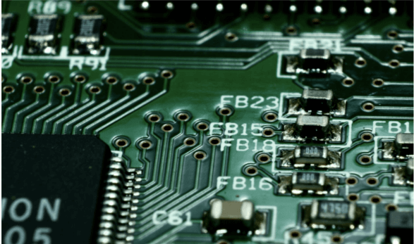
2.4 Ferrite Beads and Chokes
Ferrite beads and chokes are passive components that are used to suppress high-frequency noise on power and signal lines. They work by absorbing electromagnetic energy and converting it into heat. Ferrite beads are typically placed on individual traces, while ferrite chokes are used on cables and connectors.
2.5 Shielding Gaskets
Shielding gaskets are used to create a conductive seal between two surfaces, such as a PCB and its enclosure. They are made from materials like conductive elastomers or metal-filled polymers and are designed to fill gaps and irregularities, ensuring a continuous conductive path that blocks EMI.
2.6 Via Fencing
Via fencing involves placing a series of vias (plated through-holes) around the perimeter of a sensitive area on the PCB. These vias are connected to the ground plane, creating a “fence” that helps to contain electromagnetic fields and prevent them from radiating outward.
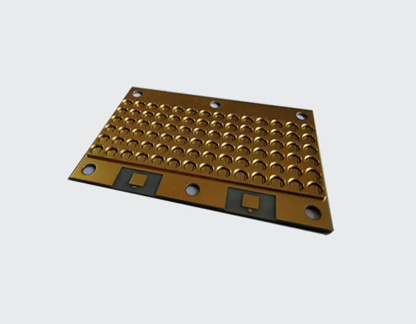
2.7 Embedded Shielding
Embedded shielding involves integrating shielding materials directly into the PCB substrate. This can be achieved by using conductive layers or meshes within the PCB stack-up. Embedded shielding provides a more compact and integrated solution compared to external shielding methods.
3. Design Considerations for Effective PCB Shielding
3.1 Component Placement
Proper placement of components on the PCB is crucial for effective shielding. Sensitive components should be placed away from potential sources of EMI, such as high-speed digital circuits or power supplies. Grouping related components together can also help to minimize the area that needs to be shielded.
3.2 Layer Stack-up
The layer stack-up of a PCB plays a significant role in its shielding effectiveness. A well-designed stack-up should include dedicated ground and power planes, which help to reduce EMI and improve signal integrity. The use of multiple ground planes can further enhance shielding by providing additional paths for return currents.
3.3 Trace Routing
Careful routing of traces is essential to minimize crosstalk and EMI. High-speed signals should be routed away from sensitive analog circuits, and differential pairs should be routed close together to reduce electromagnetic radiation. The use of controlled impedance traces can also help to maintain signal integrity.
3.4 Shielding Material Selection
The choice of shielding material depends on the specific requirements of the application. Factors to consider include the frequency range of the EMI, the mechanical properties of the material, and the environmental conditions in which the PCB will operate. Conductive coatings, for example, are suitable for high-frequency applications, while shielding cans provide robust physical protection.
3.5 Thermal Management
Shielding can impact the thermal performance of a PCB by trapping heat generated by components. It is important to consider thermal management techniques, such as the use of thermal vias, heat sinks, and proper ventilation, to ensure that the PCB operates within its temperature limits.
4. Testing and Validation of PCB Shielding
4.1 EMI Testing
EMI testing is conducted to evaluate the effectiveness of the shielding techniques employed in a PCB. This involves measuring the levels of electromagnetic radiation emitted by the PCB and comparing them to regulatory limits. Common EMI testing methods include radiated emissions testing and conducted emissions testing.
4.2 Signal Integrity Testing
Signal integrity testing is performed to ensure that the electrical signals on the PCB are not degraded by EMI or other factors. This can involve measuring parameters such as rise time, fall time, and jitter, as well as performing eye diagram analysis to assess the quality of high-speed signals.
4.3 Environmental Testing
Environmental testing is conducted to evaluate the performance of the PCB under various environmental conditions, such as temperature, humidity, and vibration. This helps to ensure that the shielding remains effective and that the PCB operates reliably in its intended environment.
5. Advanced PCB Shielding Techniques
5.1 Active Shielding
Active shielding involves the use of active components, such as amplifiers and filters, to counteract EMI in real-time. This technique is particularly useful in applications where traditional passive shielding methods are insufficient, such as in high-frequency or high-power circuits.
5.2 Frequency-Selective Shielding
Frequency-selective shielding involves the use of materials or structures that selectively block or attenuate specific frequency ranges. This can be achieved using metamaterials or frequency-selective surfaces (FSS), which are designed to interact with electromagnetic waves in a controlled manner.
5.3 3D Shielding
3D shielding involves the use of three-dimensional structures to provide comprehensive EMI protection. This can include the use of shielding cans with complex geometries, or the integration of shielding materials into the PCB substrate in a three-dimensional arrangement.
6. Case Studies: PCB Shielding in Real-World Applications
6.1 Consumer Electronics
In consumer electronics, such as smartphones and tablets, PCB shielding is essential to ensure reliable operation and compliance with EMC regulations. Shielding cans and conductive coatings are commonly used to protect sensitive components, such as RF modules and processors, from EMI.
6.2 Automotive Electronics
Automotive electronics operate in a harsh electromagnetic environment, with potential sources of EMI including the engine, alternator, and other electronic systems. PCB shielding in automotive applications often involves the use of shielding cans, ferrite beads, and robust ground planes to ensure reliable operation.
6.3 Medical Devices
Medical devices, such as MRI machines and pacemakers, require high levels of EMI protection to ensure patient safety and device reliability. PCB shielding in medical devices often involves the use of embedded shielding and advanced materials, such as conductive polymers, to provide effective EMI protection.
7. Future Trends in PCB Shielding
7.1 Miniaturization
As electronic devices continue to shrink in size, the need for compact and integrated shielding solutions will increase. This will drive the development of new materials and techniques, such as embedded shielding and 3D shielding, that can provide effective EMI protection in a smaller footprint.
7.2 Higher Frequencies
The trend towards higher operating frequencies, driven by technologies such as 5G and the Internet of Things (IoT), will require more advanced shielding techniques to manage EMI at these frequencies. Frequency-selective shielding and active shielding are likely to play a key role in addressing these challenges.
7.3 Sustainability
There is a growing focus on sustainability in electronics manufacturing, and this extends to PCB shielding. The development of environmentally friendly shielding materials, such as biodegradable conductive polymers, will be an important area of research in the coming years.
Conclusion
PCB shielding is a critical aspect of modern electronic design, ensuring signal integrity, preventing EMI, and maintaining EMC. A wide range of shielding techniques is available, from conductive coatings and shielding cans to advanced methods like active shielding and frequency-selective shielding. As electronic devices continue to evolve, the need for effective and innovative PCB shielding solutions will only grow. By understanding the principles of PCB shielding and staying abreast of emerging trends, designers can ensure that their products meet the highest standards of performance and reliability.