PCB signal integrity design and test application
The rapid development of high-frequency and high-speed electronic products requires PCBs to have high-performance system structures, not just supporting electronic components. The current electronic system design generally has a signal frequency higher than 100 MHz, and the high-frequency and high-speed printed circuit boards used for signal transmission are increasingly susceptible to signal integrity issues. The signal transmission process is more prone to signal integrity problems such as reflection and crosstalk, and the higher the frequency and the faster the transmission rate, the more serious the signal loss. How to reduce the loss of signals during transmission and ensure signal integrity is a huge challenge in the development of high-frequency and high-speed PCBs. In the high-frequency era, the signal integrity of PCB products is improved by PCB raw materials and PCB design products. The electrical properties of PCB materials can be measured by testing the dielectric constant, dielectric loss and conductor copper foil roughness value of the dielectric layer; the electrical properties of PCB products are mainly measured by testing impedance and insertion loss (transmission loss). It mainly introduces the dielectric constant, dielectric loss and conductor copper foil roughness test of the dielectric layer of PCB raw materials, as well as the design and test application of PCB product impedance and insertion loss.
5G, Internet of Things and unmanned driving technology are all in a stage of rapid development, and need to transmit signals under high-frequency and high-speed conditions. PCB (Printed Circuit Board) system needs to become a high-performance system structure, not just a supporting electronic component. At present, the signal frequency of electronic system design is generally higher than 100 MHz, and the high-frequency and high-speed printed circuit boards used for signal transmission are increasingly susceptible to signal integrity issues. The signal transmission process is more prone to signal integrity problems such as reflection and crosstalk, and the higher the frequency and the faster the transmission rate, the more serious the signal loss. How to reduce the signal loss during transmission and ensure signal integrity is a huge challenge in the development of high-frequency and high-speed PCB.
In the high-frequency era, the signal integrity electrical performance of PCB products is improved from two parts: PCB raw materials and PCB design products. The electrical performance of PCB materials can be measured by testing the dielectric constant (D k), dielectric loss (D f) of the dielectric layer, and the roughness value of the conductor copper foil; the electrical performance of PCB products is mainly measured by testing impedance and insertion loss (transmission loss).
This article mainly introduces the dielectric constant, dielectric loss and conductor copper foil roughness test of the dielectric layer of PCB raw materials, as well as the design and test application of PCB product impedance and insertion loss.
1 Introduction and testing of parameters of dielectric layer of PCB raw materials
1.1 D k , D f and testing of dielectric layer of PCB raw materials
1.1.1 Dielectric constant (D k ) and dielectric loss (D f )
Dielectric constant: If a material can store electrical energy when subjected to an external electric field, it is called a “dielectric”. For example, a capacitor can store charge, and when the middle of the capacitor plate is filled with a dielectric, more charge will be stored. The larger the dielectric constant, the more charge can be stored, and the greater the ability to hinder signal transmission.
Dielectric loss: In an alternating electric field, due to the hysteresis effect of dielectric conductivity and dielectric polarization, the insulating material or dielectric produces a certain phase difference between the current phasor and the voltage phasor flowing through the dielectric, that is, a certain phase angle is formed. The tangent value of this phase angle is the loss factor Df. The energy loss caused by the hysteresis effect of dielectric conductivity and dielectric polarization is called dielectric loss. In other words, the higher the Df, the more obvious the hysteresis effect of dielectric conductivity and dielectric polarization, and the more power loss or signal loss. It is a physical quantity that characterizes the power loss capacity of dielectrics and the signal loss capacity of insulating materials. Therefore, the lower the Dk and Df of the dielectric layer of the PCB material, the lower the insertion loss of the manufactured PCB product.
1.1.2 SPDR (Split Post Dielectric Resonator) method to test Dk and Df
There are many methods to test the electrical properties of high-frequency materials, including transmission line method, free space method, coaxial probe method and resonant cavity method. Among them, the resonant cavity method is the most suitable for testing low-loss materials. SPDR is one of the separated dielectric resonant cavity methods, which is a low-loss test method for a single frequency point. The structure of SPDR uses extremely low-loss dielectric materials, which enables it to build resonators with higher Q factors and better thermal stability than traditional all-metal cavities. The main advantages of SPDR are:
1) It has excellent accuracy compared to the transmission reflection method;
2) It can test low-loss materials (transmission reflection technology cannot test materials with lower losses);
3) No special sample preparation is required, and substrates and dielectric layers can be conveniently and quickly tested non-destructively.
The SPDR method is a non-destructive test method. By measuring the change in the resonant frequency and Q value before and after the dielectric layer is inserted into the resonator, the D k and D f values are tested. The test fixture and test principle are shown in Figure 1. Use different resonators for different frequencies. The SPDR fixture currently provided can cover from 1.1 GHz to 15 GHz.
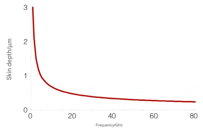
Figure 1 Relationship between skin depth and frequency 1.2 Test of conductor copper foil roughness
1.2.1 Skin effect of conductor copper foil
Under high-frequency and high-speed conditions, signal transmission is increasingly concentrated on the “surface” of the conductor, namely the skin effect. When the frequency reaches 1 GHz, the skin depth of the signal on the conductor surface is only 2.10 µm; when the signal transmission frequency is increased to 10 GHz, the skin depth of the signal on the conductor surface is 0.66 µm; and in the millimeter wave frequency band (>30 GHz), the skin depth is further reduced to below 0.40 µm (as shown in Figure 1). If the surface roughness of the conductor is greater than the skin depth, the signal transmission is only carried out within the thickness range of the roughness, making the standing wave and reflection of the transmission signal more and more serious, and causing the signal transmission path to become longer, increasing the transmission loss (as shown in Figure 2). When the surface roughness of the conductor is lower than the skin depth, the signal transmission path is short, reducing the transmission loss (as shown in Figure 3). Therefore, the lower the roughness of the conductor copper foil, the lower the insertion loss (transmission loss) of the produced PCB product.
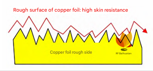
Figure 2 Signal transmission on the surface of copper foil with high roughness
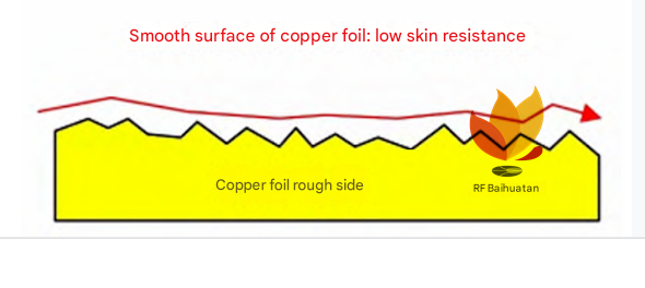
Figure 3 Signal transmission on the surface of copper foil with low roughness
1.2.2 Roughness test
The test parameters of conventional roughness are:
1) Line roughness: Ra, Rz, Rq;
2) Surface roughness: Sa, Sz, Sq, Sdr.
The definitions of Ra, Rz, Rq and Sa, Sz, Sq are the same as those of conventional roughness. Here, Sdr roughness should be emphasized.
Sdr is the interface expansion area ratio. The expansion area (surface area) of the defined area indicates how much the area has increased relative to the defined area. As shown in Figure 4, the calculation formula is:
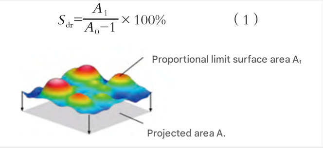
Figure 4 Definition of S dr
Why do we need to measure S dr? As shown in Figure 5, the measured Sa values of sample 1 and sample 2 are the same. After measuring S dr, it can be found that the surface roughness of sample 2 is larger.
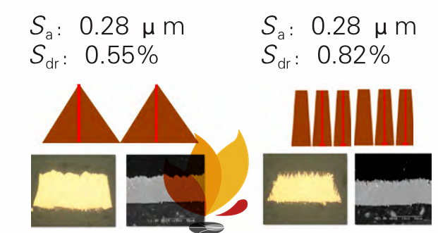
Figure 5 Samples with the same Sa value have different S dr
2 PCB product impedance design and test applications
2.1 PCB product impedance design
2.1.1 Microstrip and stripline design As shown in Figure 6, microstrip is a transmission line distributed on the outer layer of the circuit board, separated from a single ground plane by dielectric material. The design features of microstrip are:
1) The electric field penetrates two different dielectric layers, making it difficult to control impedance;
2) The dielectric constant of air is lower than that of PCB, so the dielectric constant of the overall microstrip line is lower;
3) The width of the controlled impedance trace is wider;
4) Because it is on the surface of the PCB, it is more susceptible to external interference.
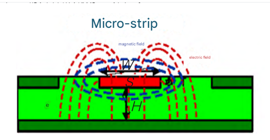
Figure 6 Microstrip line
As shown in Figure 7, the stripline is a transmission line surrounded by dielectric material, between two ground planes on the inner layer of the PCB. The design features of the stripline are:
1) The electric field is only within the PCB range, and it is easier to control the impedance;
2) The dielectric constant is higher;
3) The width of the controlled impedance trace is smaller than the width of the trace under the same impedance in the microstrip line. This is because there is a second ground plane. These smaller trace widths can achieve higher wiring density;
4) Because it is inside the PCB, it is not easily interfered.
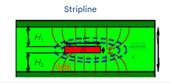
Figure 7 Stripline
Therefore, when designing samples, it is recommended to use a stripline design, which is easy to control impedance and has stronger resistance to external interference.
2.1.2 Single-point and differential design
For stripline, there is no far-end noise if the differential matching is good. Compared with single-point signals, differential signals have many advantages in signal integrity. For example, they have better noise immunity and are insensitive to attenuation. They are increasingly used in high-frequency circuit design. Key signals in the circuit often use differential structure design, as shown in Figures 8 and 9.
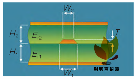
Figure 8 Single-point (single trace)
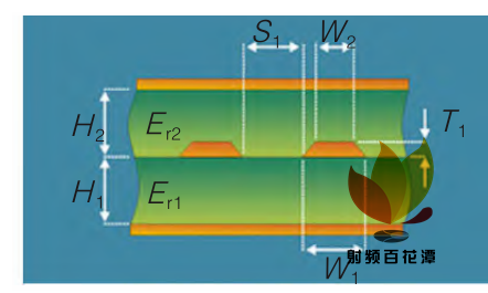
Figure 9 Differential (double trace)
2.2 PCB product impedance test 2.2.1 Impedance control
In order to make the circuit board move towards high density, small size and single component trend, when assembling high-speed components on multi-layer boards, the “characteristic impedance” of the signal line must be controlled within a certain range to ensure smooth transmission of high-frequency signals and reduce line transmission resistance, reflection, distortion, interference and other problems. This quality requirement is called “impedance control” (generally single-point impedance is controlled at 50 Ω, differential impedance is controlled at 100 Ω).
2.2.2 Impedance test
There are 3 types of impedance test equipment: 1) impedance tester; 2) oscilloscope; 3) network analyzer.
The higher the bandwidth frequency of the impedance test equipment, the narrower the rising width of the step signal it forms, and the higher the impedance test accuracy.
3 PCB product insertion loss design and test application
3.1 PCB product insertion loss design
3.1.1 High-frequency product routing design
At low frequencies, the glass fiber cloth has little effect on the electrical properties of the PCB, and the medium can be considered uniform, but at high frequencies, the local characteristics of the dielectric layer will have a great impact on the electrical properties of the PCB. Because the relative dielectric constant of the glass fiber cloth is quite different from that of the epoxy resin (epoxy resin is about 3, and glass fiber cloth is about 6), there are differences in the dielectric constants at different positions on the board surface, resulting in differences in impedance at different positions on the board surface. At the same time, the dielectric constant of the same impedance line is also uneven due to different positions, and the impact on the differential is more obvious, as shown in Figures 10 and 11. Some possible solutions to the above phenomenon are:
1) Avoid the braiding spacing of glass fiber bundles when routing;
2) Avoid the braiding spacing of glass fiber bundles when the differential routing spacing just avoids the braiding spacing of glass fiber bundles;
3) Zigzag routing;
4) Routing with a certain angle (usually 15° tilt);
5) Designers rotate the design;
6) PCB manufacturers rotate the substrate;
7) Use high-end substrate materials;
8) Use tighter glass fiber materials (small braiding spacing of glass fiber bundles).
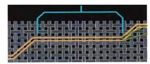
Figure 10 Incorrect high-frequency routing
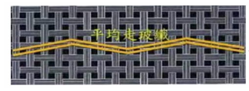
Figure 11 Correct high-frequency routing
3.1.2 De-embedding design
As shown in Figure 12, in order to eliminate test errors and via effects, three transmission lines of different lengths are designed. Generally, the lengths of the transmission lines are designed to be 2 inches (1 inch = 25.4 mm), 5 inches, and 10 inches. Insertion loss is tested by using two groups of adjacent long and short lines. The insertion loss value of the pure line can be obtained by subtracting the two groups of data and dividing by the length difference. The difference between the two groups of insertion loss data can be compared to determine the accuracy of the insertion loss of this test. That is, the insertion loss values of structures A, B, and C are the sum of their respective transmission line insertion loss values and via insertion loss values.
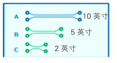
Figure 12 De-embedding design
The insertion loss value of each inch of transmission line is:

The insertion loss value of each structure is:

If the insertion loss values of the two groups of transmission lines
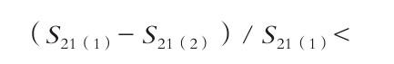
are 10%, it means that the accuracy of the insertion loss value of this test is normal.
3.1 Insertion loss test of PCB products 3.1.1 Insertion loss
Refers to the ratio of the output power of the output port to the input power of the input port.
Defined as:
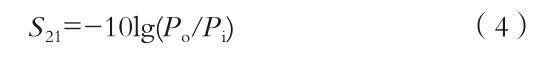
Where: Pi is the power input to the input port; Po is the power received from the output port.
3.2.2 Signal integrity
In order to meet signal integrity, before testing the electrical performance insertion loss, the product impedance must be tested to match 50 Ω or 100 Ω. This is related to the design of the electrical performance Loss test instrument. The electrical performance Loss test instrument is generally purchased with a single-ended 50 Ω and a differential 100 Ω design. When the product impedance matches the instrument port impedance, there is almost no reflection at the test port, and the test insertion loss is accurate (as shown in Figure 13); if the product impedance does not match the instrument port impedance and is mismatched, it will This causes serious reflection at the test port when testing insertion loss, resulting in large errors in the test insertion loss and inaccurate test results (as shown in Figure 14).
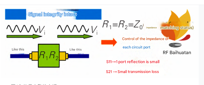
Figure 13 Signal integrity intact
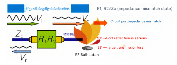
Figure 14 Signal integrity deterioration
3.2.3 Insertion loss test
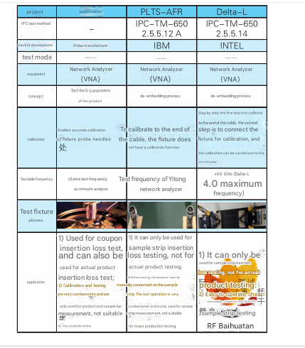
Common insertion loss test methods include the probe station method, PLTS-AFR method, and Delta-L method. Table 1 is an introduction to these three test methods.
Table 1 Three insertion loss test methods
4 Conclusion
This article briefly describes the test of signal integrity electrical performance of PCB products in the high-frequency era. The main contents include: 1) The D k , D f of the dielectric layer of PCB raw materials and the roughness test method of the conductor copper foil can directly evaluate the electrical properties of high-frequency raw materials and guide the factory to select PCB raw materials with optimal electrical performance; 2) The impedance and insertion loss design and test methods of PCB products introduce how to improve the insertion loss test accuracy through impedance design matching, and what type of insertion loss test fixture to choose as a test reference based on market demand, test frequency, ease of operation, and test accuracy.