PCB silk screen pcb technology:Priciple process and application
1. Overview of Screen Printing PCB Technology
Screen printing plays a vital role in the manufacture of printed circuit boards (PCBs). This technology provides intuitive visual guidance for electronic assembly and maintenance by printing logos, text and symbols on the surface of PCBs. Screen printing PCB technology has been developed since the mid-20th century and has become an indispensable process in the electronics manufacturing industry.
1.1 Definition of Screen Printing PCB
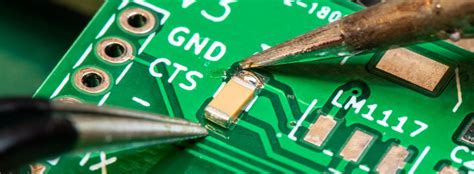
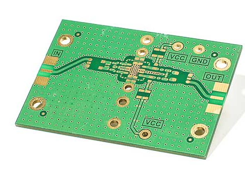
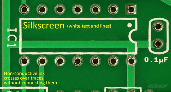
Screen printing PCB refers to the process of transferring ink to the board surface through a specific printing process on a printed circuit board with completed circuit wiring to form graphic text such as component identification, polarity marking, version information, and company logo. These printed marks are usually white, but other colors are also available. The professional term is called “Legend” or “Marking”.
1.2 Technology Development History
Screen printing technology originated from the silk-screen printing process in the Sui and Tang Dynasties in China and was introduced into the industrial field in the early 20th century. The application in the PCB industry began in the 1950s. With the miniaturization and complexity of electronic devices, screen printing PCB technology has evolved from manual operation to full automation. In recent years, with the emergence of new technologies such as inkjet printing, traditional screen printing technology has also been continuously innovated to adapt to high-precision requirements.
1.3 The role of screen printing in PCB manufacturing
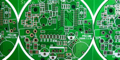
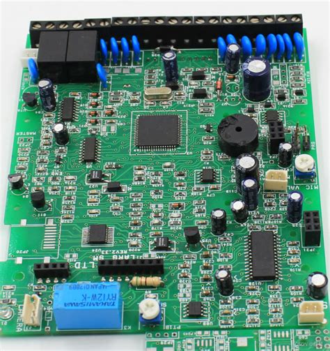
Screen printing has multiple functions in PCB manufacturing: first, it provides clear instructions for component location and orientation to prevent assembly errors; second, it contains information such as version numbers and serial numbers to facilitate product tracking; third, it adds warning symbols and safety logos to meet safety regulations; finally, the printing of brand logos also enhances the professionalism and recognition of the product.
2. The process flow of screen printing PCB
Screen printing PCB is a multi-step precision process, and each link directly affects the final printing quality. The standard process flow is introduced in detail below.
2.1 Preliminary preparation
Design file processing: Extract the silk screen layer information from the Gerber file, and use special software (such as CAM350) for graphic processing and typesetting optimization. Designers need to ensure that the text size matches the board space. Usually, the minimum character height is recommended to be no less than 0.8mm.
Screen production: Select a stainless steel or polyester screen with an appropriate mesh size (usually 120-200 mesh), apply photosensitive glue, and then form a pattern through exposure and development. High-precision printing requires a fine mesh of more than 350 mesh, and the film thickness is controlled at 10-15μm.
PCB board surface processing: Clean the board surface to remove the oxide layer and contaminants, and perform micro-etching if necessary to enhance the ink adhesion. For special surfaces (such as immersion gold, tin spraying), corresponding pre-treatment processes are required.
2.2 Printing process
Ink selection: Commonly used epoxy resin inks need to consider high temperature resistance (usually need to withstand 288℃/10s welding temperature), insulation performance (>10^8Ω) and environmental protection requirements (RoHS compliance). UV curing inks are becoming increasingly popular due to their high production efficiency.
Printing parameter control: The scraper angle is usually set at 60-75°, the pressure is controlled at 0.3-0.5MPa, and the printing speed is maintained at 10-30cm/s. These parameters need to be adjusted according to the ink characteristics and pattern fineness.
Positioning accuracy: Modern fully automatic screen printers use CCD visual positioning systems, which can achieve ±25μm alignment accuracy, meeting the strict requirements of high-density interconnect (HDI) boards.
2.3 Post-processing process
Curing process: Thermal curing inks are usually baked at 150℃ for 15-30 minutes, while UV inks require 300-400mJ/cm² of ultraviolet light. Insufficient curing will lead to poor adhesion, while over-curing may cause brittle cracking.
Quality inspection: including visual inspection (missing printing, blurring, offset, etc.), adhesion test (3M tape method) and chemical resistance test (flux, cleaning agent immersion). The automatic optical inspection (AOI) system can realize rapid screening of printing defects.
Rework process: For unqualified printing, special solvents (such as dimethylformamide) can be used to remove the ink without damaging the substrate, and reprint after cleaning.
3. Technical points of screen printing PCB
3.1 Material selection
Ink performance parameters:
- Viscosity: 3000-10000cps (25℃)
- Fineness: ≤15μm
- Hardness: ≥4H (pencil hardness)
- Insulation resistance: ≥10^12Ω·cm
** Screen parameter comparison**:
| Screen type | Mesh number | Line diameter (μm) | Opening rate (%) | Applicable accuracy |
|---|---|---|---|---|
| Standard screen | 120-150 | 50-70 | 35-45 | ≥0.2mm line width |
| Fine mesh | 180-230 | 34-48 | 30-35 | 0.15-0.2mm |
| Extra fine mesh | 300-400 | 18-34 | 15-25 | ≤0.1mm |
3.2 Key points of process control
Environmental control: The temperature should be maintained at 23±3℃ and the relative humidity should be 40-60%. Excessive humidity will cause the ink to absorb moisture and affect curing, while temperature fluctuations will cause changes in ink viscosity.
Thickness control: The dry film thickness is usually controlled at 15-25μm. Too thin will affect the hiding power, and too thick will easily cause cracks. The film thickness meter can be used to measure to ensure consistency.
Resolution improvement: The indirect plate making method can achieve a line width resolution of 50μm, while the electroforming screen can achieve ultra-fine printing of 25μm.
3.3 Common problems and solutions
Printing defect analysis:
- Ink seepage: The reasons include too thin ink, insufficient screen tension (should be maintained at 20-25N/cm) or excessive scraper pressure. Solutions include adjusting ink viscosity, replacing high-tension screens, and optimizing scraper parameters.
- Jagged edges: Usually related to insufficient screen resolution or the slope of the photosensitive adhesive edge. The use of capillary photosensitive film can significantly improve edge quality.
- Poor adhesion: May be caused by board surface contamination or incomplete curing. It is recommended to strengthen pre-treatment and verify whether the curing curve meets the standard.
Special substrate response:
- Flexible PCB: Use elastic modified epoxy ink, and the curing temperature does not exceed 130℃
- Metal substrate: Special high-temperature ink is required (temperature resistance>300℃)
- High-frequency material: Use low dielectric constant ink (Dk<3.5)
4. Technical innovation of screen printing PCB
4.1 New printing technology
Laser direct imaging (LDI): Eliminates the screen production process and directly forms ink patterns on the PCB surface through laser. The resolution can reach 20μm, which is suitable for small batch and multi-variety production.
Digital inkjet printing: piezoelectric nozzles are used to precisely spray ink to the designated position to achieve contactless printing, which is especially suitable for uneven surfaces. The minimum feature size can currently reach 50μm.
3D curved surface printing: precise printing on three-dimensional structured PCBs is achieved through special fixtures and flexible screens to meet special application requirements such as automotive electronics.
4.2 Environmentally friendly materials
Water-based ink: VOC content is less than 5%, and it is cured by water evaporation and cross-linking reaction, and requires special drying equipment.
UV-LED curing: compared with traditional mercury lamps, energy consumption is reduced by 70%, and it does not contain ozone, and the working life is more than 20,000 hours.
Bio-based resin: plant extracts are used to replace petroleum-derived ingredients, reducing carbon footprint by 40%, while maintaining excellent heat resistance.
4.3 Intelligent production
Internet of Things monitoring: sensors are integrated in printing equipment to collect parameters such as temperature, humidity, and pressure in real time, and process traceability is achieved through the MES system.
AI quality prediction: Analyze historical data based on machine learning algorithms, warn of potential defects in advance, and reduce the defect rate.
Adaptive control system: Automatically adjust printing parameters according to board thickness and material, shortening line change time by more than 30%.
5. Application and development of screen-printed PCB
5.1 Current status of industry applications
Consumer electronics: Smartphone motherboards require ultra-high precision screen printing below 0.1mm, and wearable devices such as Apple Watch require three-dimensional printing technology.
Automotive electronics: PCB screen printing of engine control units (ECUs) must withstand temperature cycles and vibration environments from -40℃ to 150℃.
Medical equipment: PCB logos for implantable devices must use biocompatible inks and pass ISO 10993 certification.
Aerospace: The screen printing materials of satellite PCBs must withstand cosmic rays and extreme temperatures, and special ceramic filler inks are usually used.
5.2 Technology Development Trends
Adaptation to high-density interconnection: As PCB line width/spacing develops toward 50/50μm, screen printing technology needs to simultaneously improve accuracy and develop new nano-inks.
Multifunctional integration: Develop smart inks with insulation, heat dissipation and electromagnetic shielding functions to reduce subsequent processing steps.
Green manufacturing: Halogen-free and heavy metal-free inks will become the mainstream, and zero wastewater discharge will be achieved with a closed-loop cleaning system.
Flexible electronic support: Develop stretchable inks (elongation>100%) to meet the needs of flexible displays and wearable devices.
5.3 Future challenges and opportunities
Micro-fining challenges: When the feature size is less than 30μm, traditional screen printing faces physical limits and needs to be combined with processes such as lithography.
New material development: The printing application of new conductive materials such as graphene and carbon nanotubes will open up new possibilities.
Cross-industry integration: Learn from technological innovations in fields such as textile printing and glass decoration to enrich the expression of PCB printing.
Personalized customization: Digital printing technology makes it possible to personalize PCB logos in small batches, meeting the needs of makers and prototype development.

Conclusion
As a basic process in the field of electronic manufacturing, screen printing PCB technology has matured, but it is still innovating driven by new materials and new demands. From traditional large-scale standardized production to today’s precision printing for flexible electronics and IoT devices, screen printing technology continues to demonstrate its adaptability and vitality. In the future, with the development of industries such as 5G, artificial intelligence and new energy, PCB screen printing technology will evolve towards higher precision, more environmentally friendly and smarter directions, and continue to provide reliable guarantees for the functional realization and quality improvement of electronic products. Manufacturing companies should pay close attention to technological development trends and increase R&D investment to maintain their dominant position in the increasingly fierce market competition.