PCB Silkscreen: A Comprehensive Guide
Introduction to PCB Silkscreen
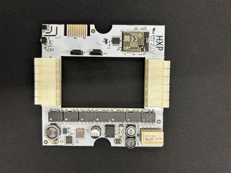
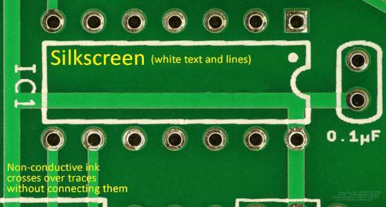
Printed Circuit Board (PCB) silkscreen, often referred to as “legend printing,” is a critical layer in PCB manufacturing that provides essential visual information on the board. The silkscreen layer includes component designators, polarity markers, logos, part numbers, and other annotations that help in assembly, debugging, and maintenance.
Silkscreen printing is typically applied using different methods, including liquid photo imaging (LPI), direct legend printing (DLP), and traditional screen printing. Each technique has its advantages and limitations, depending on the PCB’s complexity, resolution requirements, and cost considerations.
This article explores the purpose of PCB silkscreen, the different printing methods, design considerations, and best practices to ensure high-quality and functional silkscreen layers.
Purpose of PCB Silkscreen
The primary functions of PCB silkscreen include:
- Component Identification
- Labels such as R1, C2, U3 help assemblers place components correctly.
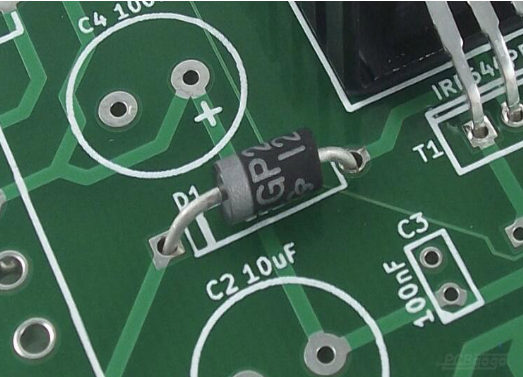
- Polarity indicators (e.g., “+,” “−,” diode markings) prevent reverse insertion.
- Assembly and Debugging Assistance
- Test points, pin numbers, and reference designators aid in troubleshooting.
- Company logos, version numbers, and certifications (e.g., CE, UL) provide traceability.
- User Guidance
- Connector labels (e.g., “USB,” “PWR”) improve usability.
- Warning symbols (e.g., high-voltage areas) enhance safety.
- Aesthetic and Branding
- Custom logos, product names, and serial numbers enhance brand recognition.
Silkscreen Printing Methods
1. Traditional Screen Printing
- Process: A stencil (mesh screen) is used to apply ink onto the PCB.
- Resolution: Limited to ≥0.007″ (0.18mm) line width.
- Best for: Low-cost, large-text PCBs with simple designs.
- Limitations: Poor for fine-pitch components.
2. Liquid Photo Imaging (LPI)
- Process: A photosensitive ink is applied, exposed to UV light, and developed.
- Resolution: Supports ≥0.004″ (0.1mm) line width.
- Best for: High-density PCBs with small components.
- Advantages: Higher accuracy than screen printing.
3. Direct Legend Printing (DLP)
- Process: Inkjet printing with acrylic ink cured by UV light.
- Resolution: ≥0.003″ (0.075mm), suitable for ultra-fine text.
- Best for: Prototyping and flexible PCBs.
- Limitations: Ink durability may be lower than LPI.
| Method | Resolution | Cost | Durability | Best Use Case |
|---|---|---|---|---|
| Screen Printing | ≥0.18mm | Low | High | Simple, large PCBs |
| LPI | ≥0.1mm | Medium | Very High | High-density PCBs |
| DLP | ≥0.075mm | High | Medium | Prototypes, fine text |
Design Considerations for PCB Silkscreen
1. Text Size and Legibility
- Minimum recommended text height: 1.0mm (for readability).
- Line width: ≥0.15mm (to prevent smudging).
- Font style: Sans-serif (e.g., Arial) for clarity.
2. Placement Guidelines
- Avoid placing silkscreen over pads, vias, or solder mask openings.
- Ensure text does not interfere with component footprints.
- Keep critical markings (polarity, pin 1) near relevant components.
3. Color Choices
- Most common: White (high contrast on green solder mask).
- Alternatives: Black, yellow, or red (depending on solder mask color).
4. International Standards
- Follow IPC-7351 for component labeling.
- Include RoHS, CE, or FCC marks if applicable.
Common Silkscreen Mistakes to Avoid
- Overlapping Solder Mask
- Silkscreen on exposed copper can lead to ink peeling.
- Incorrect Orientation
- Upside-down text makes assembly difficult.
- Excessive Clutter
- Too much text reduces readability.
- Missing Critical Markings
- Omitting polarity or pin 1 indicators causes assembly errors.
Future Trends in PCB Silkscreen Technology
- Laser Marking
- Emerging as an alternative for high-precision, permanent markings.
- 3D Printed Silkscreen
- Enables dynamic labeling for flexible PCBs.
- Smart Ink
- Conductive or UV-reactive inks for advanced applications.
Conclusion
PCB silkscreen plays a vital role in PCB manufacturing by providing essential visual cues for assembly, debugging, and usability. Choosing the right printing method (screen printing, LPI, or DLP) depends on the PCB’s complexity and cost constraints. Proper design practices—such as optimal text size, placement, and color selection—ensure clarity and functionality.
As PCB technology evolves, innovations like laser marking and smart inks will further enhance silkscreen capabilities. By adhering to industry standards and avoiding common mistakes, designers can maximize the effectiveness of the silkscreen layer, improving both manufacturability and end-user experience.