
PCB Edge Plating: Process and Applications for Grounding
When designing modular PCB systems or RF shielding enclosures, how do you create reliable electrical connections along the board edge? PCB edge plating deposits copper along the vertical sidewall of your circuit board, enabling ground continuity, EMI shielding, and direct module-to-module connections without traditional connectors.
Edge plating fundamentally changes how your PCB interfaces with enclosures, daughterboards, and RF shields. Understanding the process constraints and design rules prevents costly fabrication rework.
What Is PCB Edge Plating?
PCB edge plating creates a continuous or segmented conductive copper layer along the vertical edge of a printed circuit board. Unlike standard copper traces that exist only on horizontal surfaces, edge plating extends metallization to the Z-axis, forming electrical connections on board sidewalls.
Manufacturers achieve edge plating through two approaches: full edge metallization and castellated holes. Full edge plating applies copper continuously along an entire routed edge. Castellated holes—plated half-holes—position standard plated through-holes at the board perimeter, then route through the hole centers, leaving plated semicircular notches.
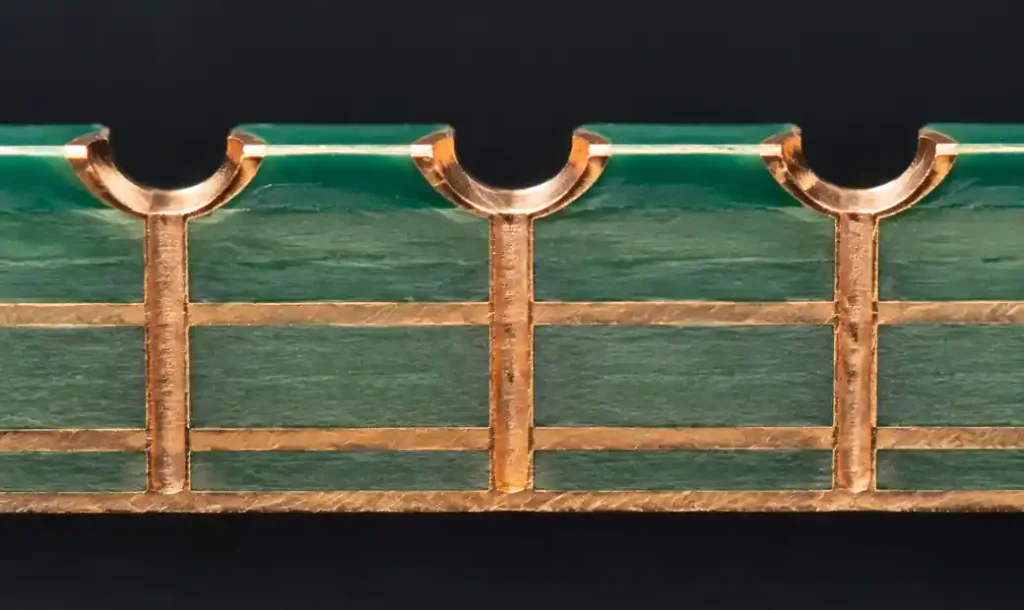
The process requires specialized fabrication steps. After initial copper etching but before final routing, manufacturers create the board outline. The exposed sidewalls undergo electroless copper deposition followed by electrolytic plating, building 18-50µm copper thickness on vertical surfaces. Finally, standard surface finish (ENIG, HASL, or immersion silver) covers the plated edges.
Edge Plating Manufacturing Process
Pre-routing occurs before copper plating for castellated designs. The manufacturer routes the board outline and drills edge holes in raw laminate. When through-hole plating occurs next, copper deposits onto exposed edge surfaces simultaneously with hole barrels, ensuring uniform 25µm minimum thickness.
Post-routing applies to full edge metallization. After completing all standard PCB processes, the manufacturer routes the final board outline. These edges then undergo separate plating operations using electroless copper initiation followed by copper build-up.
| Process Stage | Castellated Holes | Full Edge Plating | Typical Thickness |
|---|---|---|---|
| Outline Definition | Pre-routing before plating | Post-routing after PTH | N/A |
| Copper Deposition | Standard PTH process | Separate edge plating | 18-50µm |
| Surface Finish | Simultaneous with board | Separate edge finishing | 3-5µm |
| Manufacturing Time | +0 days | +1-2 days | N/A |
Most fabricators require 0.25-0.50mm clearance between the board edge and any copper feature on outer layers. This clearance prevents copper peeling and ensures plating adhesion.
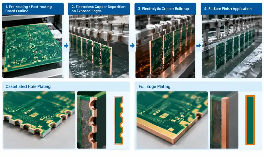
Castellated Holes vs Full Edge Plating
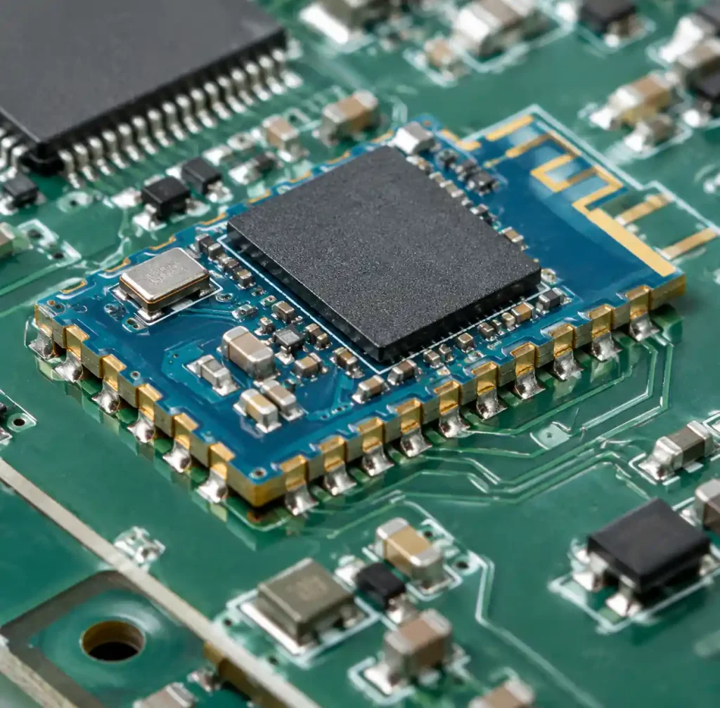
Castellated holes dominate module designs where boards mount as surface-mount components onto parent PCBs. A 20mm × 30mm WiFi module might use 24 castellations on 1.27mm pitch, providing connections without connectors that add 3-5mm height.
When you reflow solder onto castellated edges, surface tension pulls solder into the semicircular cavity, creating a fillet that mechanically locks the module to the parent board.
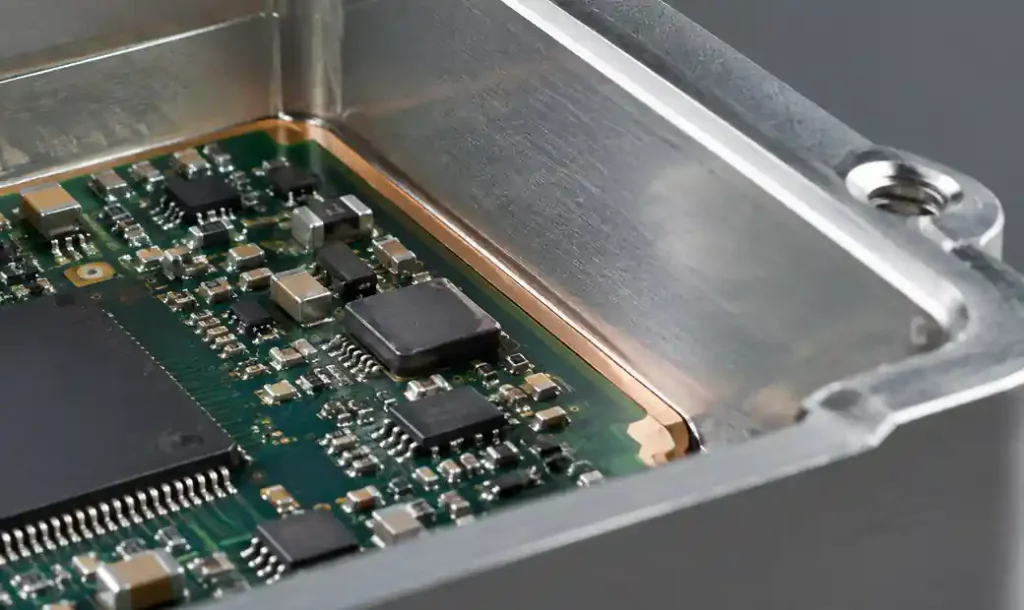
Full edge metallization serves RF shielding and chassis grounding where you need continuous conductivity. When mounting a PCB inside a metal enclosure for EMI containment, plated edges contact the case walls, creating a Faraday cage. Military modules requiring MIL-STD-461 compliance specify continuous edge plating to achieve <30dB shielding effectiveness above 1GHz.
Cost favors castellations for volume production. Castellated boards process through standard PCB manufacturing without additional operations. Full edge plating adds labor-intensive manual steps, creating 25-40% price premiums versus castellated designs below 1000 units.
Design Rules for Reliable Edge Plating
Start with minimum 0.6mm (24 mil) finished hole diameter for castellations. Smaller holes leave insufficient plated copper after routing. Standard practice uses 0.8-1.2mm diameter holes, providing 0.4-0.6mm of plated copper width—sufficient for reliable automated assembly.
For high-current ground connections, increase hole diameter to 1.5mm or use multiple castellations in parallel. Each 1.0mm castellation carries approximately 3A continuous current with 20°C temperature rise.
Castellation spacing depends on assembly method. Hand soldering tolerates 2.0mm pitch, but automated pick-and-place performs better at 2.54mm pitch or wider.
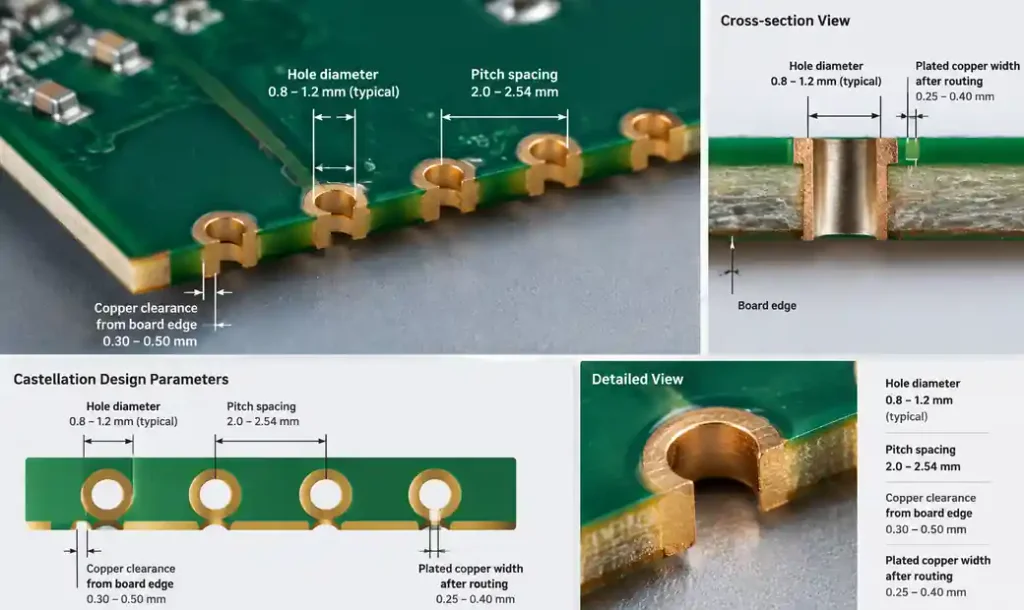
Edge-plated designs need 0.30-0.50mm clearance because the plating process adds copper thickness to edge faces, potentially creating shorts if traces run too close.
Grounding Applications and EMI Shielding
When mounting a shielded RF module inside a cast aluminum enclosure, plated edges provide dozens of low-inductance ground points. This distributed grounding topology reduces ground loop impedance, critical for noise-sensitive circuits and high-speed digital designs above 1GHz.
A single pin-to-board ground connection exhibits 10-15nH parasitic inductance. At 2.4GHz, this creates 188-282 ohms impedance—effectively an open circuit. Edge plating with continuous perimeter contact reduces equivalent inductance to <1nH, maintaining ground impedance below 15 ohms.
| Grounding Method | Inductance (nH) | Impedance @ 2.4GHz | Contact Points |
|---|---|---|---|
| Single pin header | 10-15 | 150-225Ω | 1-4 |
| Edge plating continuous | 0.5-1.0 | 7-15Ω | 20-50 |
| Castellated 2mm pitch | 2-3 | 30-45Ω | 10-20 |
| Board-to-board connector | 5-8 | 75-120Ω | 10-30 |
Testing per MIL-STD-461 shows that enclosures with edge-plated PCB gaskets achieve 35-45dB attenuation from 1-18GHz compared to 20-28dB for mechanically fastened boards without edge grounding.
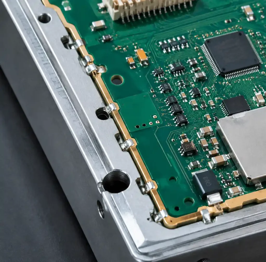
For shielding applications, specify continuous edge plating rather than castellations. Gaps between castellated holes create resonant antennas. A 15mm gap between castellations resonates near 5GHz, creating a notch in shielding effectiveness exactly where WiFi operates.
Module Edge Connector Applications
Castellated PCBs function as solderable modules, replacing traditional board-to-board connectors. Bluetooth and WiFi modules, sensor breakout boards, and processor modules use castellation because assembly height decreases by 3-8mm.
A 30-pin board-to-board connector costs $0.80-2.50 in 1000 unit quantities, plus $0.15-0.40 for the mating connector. Castellated assembly eliminates both connectors, saving $0.95-2.90 per unit. For a product shipping 50,000 units annually, this represents $47,500-145,000 in component cost reduction.
Thermal performance improves with castellated mounting because solder joints provide direct thermal conduction to the parent board’s ground plane. A metal core PCB module with 0.8W power dissipation at 85°C junction temperature drops to 65°C when the parent board includes a thermal ground plane.
Cost Factors and Lead Time
Castellated designs add minimal cost—typically 5-10% premium versus non-castellated boards in volumes above 500 units. Full edge plating requires 30-50% price increase.
A 50mm × 75mm castellated board costs $8 per piece for 10 units but drops to $2.80 at 100 units and $1.20 at 1000 units. Full edge plating: $25-35 for prototypes, $8-12 at 100 units, $3-5 at 1000 units.
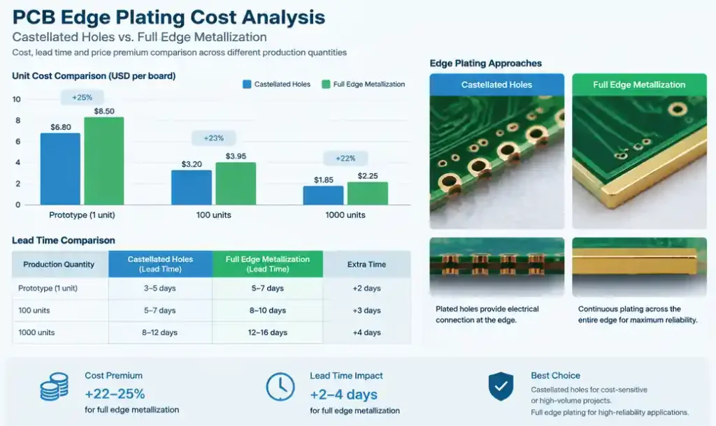
Quick turn PCB assembly providers now deliver castellated prototypes in 3-5 days.
Common Edge Plating Defects
Incomplete copper coverage represents the most frequent defect. This occurs when electroless copper initiation fails to deposit seed layer uniformly. The root cause traces to inadequate surface cleaning or resin smearing from dull router bits. Specify router bit replacement every 1000 linear inches of cutting.
Copper peeling at the board edge junction results from insufficient adhesion between horizontal and vertical copper layers. Require manufacturers to specify minimum 0.40mm copper pullback and verify that plating thickness on edges matches PTH barrel thickness within ±20%.
Castellation spacing inconsistency affects automated assembly yield. Specify routing tolerance of ±0.10mm maximum for castellated edges.
Industrial Control Applications
Industrial control PCBs with edge plating serve motor drives, PLC I/O modules, and distributed control systems. Castellated edges on 19mm × 120mm I/O cards allow field technicians to replace failed modules without soldering equipment.
Spring contacts specified for 80-120 grams force per pin maintain reliable connections across -40°C to +85°C. Design edge plating width minimum 3mm for spring contact interfaces and specify ENIG surface finish for 100,000+ insertion cycles wear resistance.
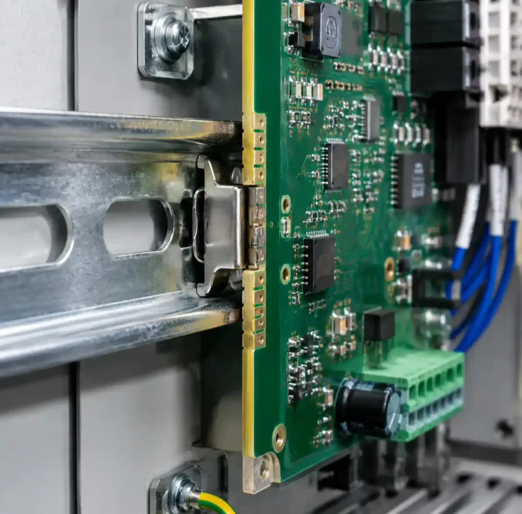
DIN rail mounting systems integrate with edge-plated PCBs for compact installations. A 100mm × 160mm controller board with continuous edge plating mounts directly to aluminum DIN rails, creating electrical ground connection through mechanical pressure, achieving <10 milliohm ground impedance.
Frequently Asked Questions
Can edge plating connect to internal layers in multilayer PCBs?
Yes, but it requires specific fabrication instructions. Standard edge plating connects only to outer layer copper within 0.5mm of the edge. To reach internal layers, specify blind or buried vias near the edge that connect your desired layers to surface pads.
What surface finishes work best for edge plating applications?
ENIG (Electroless Nickel Immersion Gold) provides optimal durability for edge contacts subject to repeated insertions. Immersion silver costs 30-40% less and works well for castellated modules that undergo one-time reflow assembly. Avoid HASL on edge plating because uneven solder coating creates inconsistent contact surfaces.
Does edge plating affect PCB impedance control for RF designs?
Edge plating changes electromagnetic boundary conditions along the board perimeter. The plated edge creates parasitic capacitance to edge-adjacent traces, lowering characteristic impedance by 3-8 ohms for traces within 1mm of the edge. Route high-speed signals minimum 2mm from plated edges.
How do I specify edge plating in Gerber files?
For castellated holes, create standard plated through-holes positioned at the board edge, with hole centers on the board outline line. Add a fabrication note: “Plated half-holes (castellations) on board edges per mechanical drawing.” For full edge plating, add: “Edge plating required on [top/bottom/both] edges, connect to ground plane, minimum 25µm thickness.”
Can I combine edge plating with rigid-flex PCB designs?
Yes, rigid-flex boards frequently use edge plating on rigid sections for grounding and module interconnection. Flexible sections cannot accommodate edge plating because polyimide film lacks mechanical structure to support copper deposition on thin edges. Design the transition between rigid and flex sections minimum 5mm from any edge plating features.
Conclusion
PCB edge plating extends circuit board connectivity beyond traditional copper layers, enabling chassis grounding, EMI shielding, and connector-free module assembly. Success depends on understanding process constraints and designing within manufacturer capabilities.
The manufacturing reality demands specific accommodations: 0.30-0.50mm copper clearance from board edges, minimum 0.6mm hole diameters for castellations, and ±0.10mm routing tolerance. These parameters directly impact electrical performance—edge grounding inductance below 1nH requires continuous plating.
Cost and lead time favor castellated designs for volume production, with 5-10% price premiums versus 30-50% for full edge plating. Quick-turn prototype services now support castellations with 3-5 day delivery. For custom applications in industrial control or automotive electronics, early manufacturer engagement prevents costly production failures.
Define electrical requirements first—ground impedance targets, shielding effectiveness, or current-carrying needs—then select castellation versus continuous plating based on those specs.