PCB Silkscreen Inversion: Causes, Impacts, and Solutions
Abstract
This paper examines the phenomenon of PCB silkscreen inversion, a common issue in printed circuit board manufacturing where the component markings and identifiers appear reversed or mirrored on the finished board. We explore the technical causes of this problem, its impact on assembly and maintenance processes, various prevention methods, and corrective approaches when inversion occurs. The discussion covers design software considerations, manufacturing workflow analysis, and quality control measures to minimize silkscreen inversion errors in PCB production.
1. Introduction
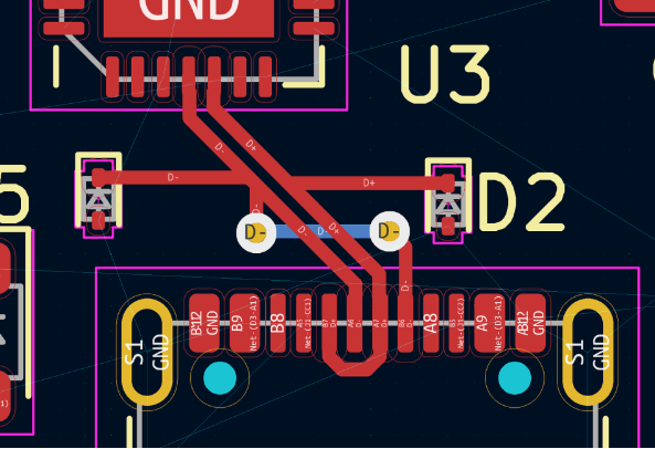
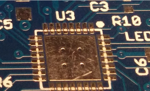
Printed Circuit Board (PCB) silkscreen, also known as legend printing, serves as the informational layer that provides critical visual references for component placement, polarity markings, part numbers, and other identifiers. Silkscreen inversion occurs when these markings appear mirrored or reversed on the final product, potentially causing assembly errors, functional issues, or maintenance challenges.
The silkscreen layer, typically printed with epoxy ink, plays several essential roles:
- Component identification and orientation
- Test point labeling
- Version control information
- Company logos and certifications
- Warning symbols and safety information
When this layer appears inverted, the consequences can range from minor inconvenience to catastrophic failure, depending on the board’s complexity and application. This paper analyzes the root causes of silkscreen inversion, its technical implications, and comprehensive solutions to prevent and address this manufacturing issue.
2. Causes of PCB Silkscreen Inversion
2.1 Design File Misalignment
The most prevalent cause of silkscreen inversion stems from inconsistencies between the design files and manufacturing processes. Several specific scenarios can lead to this problem:
Layer Stack Misinterpretation: When the PCB design software and the manufacturer’s CAM system interpret layer stacking differently, inversion may occur. This is particularly common when designers fail to properly define the layer orientation in their design files.
Gerber File Generation Errors: Incorrect Gerber file generation settings can flip the silkscreen layer. This often happens when designers:
- Select the wrong “view” option (component side vs. solder side)
- Use incorrect mirroring settings during file export
- Fail to maintain consistent layer mapping conventions
Reference Plane Confusion: Designers sometimes forget that the silkscreen must account for whether it’s being viewed from the top or bottom of the board. The increasing complexity of multi-layer boards exacerbates this challenge.
2.2 Manufacturing Process Issues
Even with correct design files, manufacturing steps can introduce inversion:
Screen Printing Process Errors: In traditional screen printing methods, improper screen preparation or mounting can cause the silkscreen to appear inverted. The emulsion side of the screen must properly align with the board orientation.
Direct Legend Printing (DLP) Misconfiguration: Modern PCB manufacturers often use inkjet-style direct printing systems. Incorrect configuration of these systems regarding board orientation can lead to inverted output.
Panelization and Step-and-Repeat Errors: When multiple boards are panelized for production, incorrect panelization settings may inadvertently mirror individual board silkscreens.
2.3 Documentation and Communication Gaps
Many silkscreen inversion issues stem from inadequate communication between design and manufacturing teams:
Missing Layer Purpose Specifications: Design files that don’t clearly indicate which side each silkscreen layer belongs to create interpretation challenges.
Incomplete Drawing Notes: Fabrication drawings that lack clear orientation markers or view specifications increase inversion risks.
Cultural Differences in View Conventions: International manufacturing partnerships may encounter different interpretation conventions for board views, leading to accidental inversion.
3. Impacts of Silkscreen Inversion
3.1 Assembly Challenges
Inverted silkscreen creates numerous problems during PCB assembly:
Component Placement Errors: Assembly technicians relying on inverted markings may place components incorrectly, leading to:
- Wrong polarity connections
- Misaligned pins or pads
- Entirely wrong component placement
Automated Assembly Issues: Pick-and-place machines using silkscreen as reference may position components incorrectly if the markings are inverted, requiring costly rework.
Rework Difficulties: Troubleshooting and repairing boards with inverted silkscreen becomes significantly more challenging, increasing labor time and potential for additional errors.
3.2 Functional and Reliability Concerns
Beyond assembly, inverted silkscreen can affect the board’s operation:
Polarity Confusion: Critical polarity markings (diodes, capacitors, ICs) appearing inverted may lead to reverse connections that:
- Cause immediate failure during power-up
- Create latent defects that manifest later
- Reduce overall product reliability
Test and Validation Problems: Testing procedures that reference silkscreen markings become unreliable, potentially causing:
- False test failures
- Undetected manufacturing defects
- Increased quality control costs
3.3 Maintenance and Service Implications
Throughout the product lifecycle, inverted silkscreen creates ongoing challenges:
Field Service Errors: Technicians performing repairs may install replacement components incorrectly based on misleading markings.
Documentation Inconsistencies: Service manuals and schematics that don’t match the actual board markings reduce maintenance efficiency and increase error rates.
Warranty and Liability Risks: Products with persistent silkscreen errors may lead to increased warranty claims and potential liability issues, especially in safety-critical applications.
4. Prevention and Solutions
4.1 Design Phase Prevention
Implementing robust design practices can eliminate most silkscreen inversion issues:
Clear Layer Naming Conventions: Adopt unambiguous layer names (e.g., “Top_Silk_CompView” instead of just “Top_Silk”) that specify the viewing perspective.
3D Visualization Checks: Utilize PCB design software’s 3D visualization features to verify silkscreen orientation before finalizing designs.
Design Rule Checks (DRC): Implement custom DRC rules that flag potential silkscreen orientation issues, including:
- Component-to-silkscreen alignment
- Polarity marking consistency
- Layer stack verification
Fabrication Notes: Include explicit orientation instructions in fabrication drawings, such as:
- View perspective annotations
- Clear top/bottom markings
- Reference designators for orientation
4.2 Manufacturing Process Controls
Manufacturers can implement several measures to prevent silkscreen inversion:
CAM Process Verification: Implement thorough CAM review steps specifically checking for:
- Layer orientation consistency
- Silkscreen-to-copper alignment
- Polarity marking correctness
First Article Inspection (FAI): Conduct comprehensive inspection of initial production units, with special attention to silkscreen orientation, before full production runs.
Standardized View Conventions: Establish and document company-wide standards for layer view interpretation to ensure consistency across all jobs.
4.3 Corrective Actions for Inverted Silkscreen
When inversion is detected, several corrective approaches exist:
Silkscreen Reapplication: For high-value boards, the existing silkscreen can be removed (typically via abrasion or chemical processes) and reapplied correctly. This approach is costly but preserves the underlying PCB.
Overprinting: In some cases, the incorrect markings can be overprinted with the correct orientation. This requires careful alignment and may affect readability.
Design Revision and Board Replacement: For severe cases or high-volume production, creating a corrected design and manufacturing new boards may be the most reliable solution despite higher initial costs.
Acceptance with Documentation: In rare cases where inversion doesn’t affect functionality (e.g., non-critical markings), the boards may be used with comprehensive documentation of the variance and clear communication to assembly teams.
5. Best Practices for Silkscreen Management
To systematically prevent silkscreen inversion issues, implement these best practices:
1. Design Standardization:
- Create and enforce company-wide PCB design standards
- Develop silkscreen templates with pre-configured layers
- Implement version-controlled design libraries
2. Pre-production Verification:
- Require design reviews focusing on layer orientation
- Generate and inspect 3D board renderings
- Conduct virtual manufacturing simulations
3. Manufacturer Qualification:
- Audit potential manufacturers’ silkscreen processes
- Review their historical quality metrics for similar work
- Establish clear communication protocols
4. Quality Control Processes:
- Implement incoming inspection for first articles
- Develop silkscreen-specific inspection criteria
- Maintain detailed quality records for continuous improvement
6. Conclusion
PCB silkscreen inversion, while seemingly a simple graphical error, can have significant consequences for PCB functionality, manufacturability, and long-term reliability. By understanding the root causes—primarily stemming from design-to-manufacturing translation errors—engineers can implement preventive measures at both the design and production stages.
The most effective approach combines clear design intent communication, rigorous verification processes, and standardized manufacturing practices. As PCB technology continues advancing with higher densities and more complex layouts, maintaining accurate silkscreen orientation becomes increasingly critical for product success.
Future developments in intelligent design software with automated orientation checks and augmented reality-assisted assembly may further reduce silkscreen-related errors. However, the fundamental need for careful attention to layer management and clear communication between design and manufacturing teams will remain essential for preventing PCB silkscreen inversion.