PCB Stackup Design and Impedance Calculation: A Comprehensive Guide
Introduction
Printed Circuit Board (PCB) stackup design and impedance calculation are critical aspects of modern electronic design, particularly for high-speed digital circuits and high-frequency analog applications. As signal speeds continue to increase and form factors shrink, proper stackup design and controlled impedance become essential for ensuring signal integrity, reducing electromagnetic interference (EMI), and maintaining overall system performance.
This article provides a comprehensive overview of PCB stackup design principles and impedance calculation methodologies. We will examine the fundamental concepts, design considerations, material selection, and calculation techniques that engineers need to master for successful high-speed PCB design.
Fundamentals of PCB Stackup Design
What is PCB Stackup?
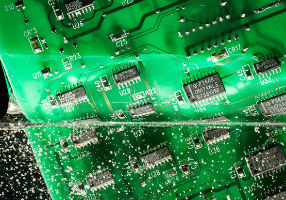
PCB stackup refers to the arrangement of copper layers and insulating materials that make up a printed circuit board. A well-designed stackup determines:
- The number of signal, power, and ground layers
- The sequence and thickness of these layers
- The dielectric materials used between layers
- The overall board thickness
Importance of Proper Stackup Design
A properly designed stackup provides numerous benefits:
- Signal Integrity: Minimizes crosstalk, reflections, and signal distortion
- Power Integrity: Provides stable power distribution with low impedance
- EMI Reduction: Contains electromagnetic fields and reduces radiation
- Manufacturability: Ensures the board can be reliably fabricated
- Cost Efficiency: Optimizes layer count and material usage
Key Considerations in Stackup Design
Layer Count Determination
The number of layers in a PCB depends on several factors:
- Circuit Complexity: More complex circuits typically require more layers
- Signal Types: High-speed signals often need dedicated layers
- Power Requirements: Multiple voltage rails may need separate layers
- Density Requirements: High component density may necessitate more layers
- Cost Constraints: More layers increase fabrication costs
A typical approach is to use even-numbered layer counts (4, 6, 8, etc.) as they generally provide better symmetry and reduce warping issues.
Layer Arrangement Strategies
Common layer arrangement strategies include:
- Signal Layers Adjacent to Ground Planes: Provides controlled impedance and return paths
- Power and Ground Plane Pairing: Creates inherent decoupling capacitance
- Cross-hatched Ground Planes: Used in some RF applications to control inductance
- Buried Signal Layers: Protects critical signals from surface noise
Symmetry Considerations
Maintaining symmetry in the stackup is crucial for several reasons:
- Mechanical Stability: Prevents warping during fabrication and assembly
- Thermal Management: Ensures even heat distribution
- Manufacturing Yield: Symmetrical designs are easier to produce reliably
Symmetry applies to both layer distribution and material thickness throughout the stackup.
Dielectric Material Selection
Common PCB Materials
The choice of dielectric material significantly affects the board’s electrical and mechanical properties:
- FR-4: The most common material, cost-effective with decent performance
- High-Frequency Laminates: (Rogers, Isola) For RF/microwave applications
- Polyimide: High temperature stability, used in flex and rigid-flex PCBs
- Ceramic-filled PTFE: Excellent high-frequency performance
Material Properties to Consider
Key material properties that influence stackup design:
- Dielectric Constant (Dk or εr): Affects signal propagation speed and impedance
- Dissipation Factor (Df or tan δ): Determines signal loss at high frequencies
- Thermal Properties: CTE, thermal conductivity, and Tg (glass transition temperature)
- Mechanical Strength: Important for reliability and manufacturing processes
Impedance Control Fundamentals
What is Controlled Impedance?
Controlled impedance means maintaining specific characteristic impedance values for transmission lines on the PCB. Common impedance values include 50Ω (single-ended), 75Ω (video), 90Ω (USB differential), and 100Ω (differential pairs like Ethernet).
Why Impedance Control Matters
Proper impedance control:
- Minimizes Reflections: Prevents signal degradation due to impedance mismatches
- Reduces EMI: Properly terminated signals radiate less electromagnetic energy
- Ensures Signal Integrity: Maintains signal quality from transmitter to receiver
- Improves Timing Accuracy: Critical for high-speed digital interfaces
Transmission Line Types
Common transmission line structures in PCBs:
- Microstrip: Signal trace on outer layer with reference plane beneath
- Stripline: Signal trace between two reference planes (internal layer)
- Coplanar Waveguide: Signal trace with adjacent ground planes on same layer
- Differential Pairs: Two closely coupled traces carrying complementary signals
Impedance Calculation Methods
Key Parameters Affecting Impedance
Several factors influence transmission line impedance:
- Trace Width (W): Wider traces lower impedance
- Trace Thickness (T): Thicker traces lower impedance
- Dielectric Thickness (H): Thicker dielectrics increase impedance
- Dielectric Constant (εr): Higher εr lowers impedance
- Solder Mask: Affects outer layer impedance (typically reduces it slightly)
Microstrip Impedance Calculation
The impedance of a microstrip transmission line can be approximated by:
For W/H ≤ 1:
Z₀ = (60/√εeff) × ln(8H/W + 0.25W/H)
For W/H > 1:
Z₀ = (120π/√εeff) / [W/H + 1.393 + 0.667ln(W/H + 1.444)]
Where εeff is the effective dielectric constant:
εeff = (εr + 1)/2 + (εr – 1)/2 × 1/√(1 + 12H/W)
Stripline Impedance Calculation
For a symmetric stripline (trace centered between planes):
Z₀ = (30π/√εr) × b/(W + 0.441b)
Where b is the total dielectric thickness between planes.
For asymmetric stripline (trace closer to one plane), more complex calculations are needed.
Differential Impedance Calculation
Differential impedance depends on:
- The single-ended impedance of each trace
- The coupling between the traces
- The spacing between the traces (S)
A simplified approximation:
Zdiff ≈ 2 × Z₀ × (1 – 0.48 × e^(-0.96×S/H))
Using Field Solvers
While these equations provide reasonable estimates, modern designs typically use:
- 2D Field Solvers: For basic cross-sectional analysis
- 3D Full-wave Solvers: For complex structures and edge cases
- Manufacturer’s Calculators: Many PCB vendors provide online tools
Practical Stackup Design Examples
4-Layer Stackup
A typical 4-layer stackup might be arranged as:
- Top Layer (Signal)
- Ground Plane
- Power Plane
- Bottom Layer (Signal)
This provides good signal integrity with reasonable cost.
6-Layer Stackup
A common high-speed 6-layer configuration:
- Top Layer (Signal)
- Ground Plane
- Signal Layer (High-speed)
- Signal Layer (High-speed)
- Power Plane
- Bottom Layer (Signal)
This provides dedicated routing layers for high-speed signals between reference planes.
8-Layer Stackup
An advanced 8-layer stackup might be:
- Top Layer (Signal)
- Ground Plane
- Signal Layer (High-speed)
- Power Plane
- Ground Plane
- Signal Layer (High-speed)
- Power Plane
- Bottom Layer (Signal)
This offers excellent signal integrity and power distribution for complex designs.
Manufacturing Considerations
Tolerance Control
Key manufacturing tolerances that affect impedance:
- Trace Width: Typically ±10-20% depending on fabrication capabilities
- Dielectric Thickness: Usually ±10% for standard materials
- Copper Thickness: Varies based on plating processes
Impedance Testing
Manufacturers typically verify impedance using:
- Time Domain Reflectometry (TDR): Measures actual impedance profile
- Coupon Testing: Tests specially designed test structures on panel edges
Design for Manufacturing (DFM)
To ensure reliable impedance control:
- Provide Clear Specifications: Document all impedance requirements
- Include Test Coupons: Allow for manufacturing verification
- Consult with Fabricator Early: Discuss stackup and material options
- Consider Panelization Effects: Impedance may vary across large panels
Advanced Topics
Mixed Dielectric Stackups
Some designs use different materials in the stackup:
- High-Speed Surface Layers: With low-Dk materials for critical signals
- Standard Core Materials: For less critical layers to reduce cost
High-Density Interconnect (HDI)
HDI designs with microvias and thin dielectrics present special challenges for impedance control.
Frequency-Dependent Effects
At very high frequencies (>10GHz):
- Dispersion: εr becomes frequency-dependent
- Surface Roughness: Affects conductor losses
- Anisotropy: Material properties vary by direction
Conclusion
PCB stackup design and impedance calculation are essential skills for modern electronic design engineers. A well-designed stackup provides the foundation for signal integrity, power integrity, and EMC performance, while proper impedance control ensures reliable signal transmission in high-speed applications.
By understanding the fundamental principles, calculation methods, and manufacturing considerations presented in this article, designers can create robust PCB layouts that meet performance requirements while remaining manufacturable and cost-effective. As signal speeds continue to increase, mastery of these concepts will only grow in importance for successful electronic product development.
Remember that while the theoretical calculations provide a good starting point, close collaboration with PCB manufacturers and the use of advanced simulation tools are often necessary to achieve optimal results in complex designs. Always verify your stackup and impedance assumptions with your fabrication partner before finalizing the design.