PCB Stage Routing Principles: A Comprehensive Guide
Introduction
Printed Circuit Board (PCB) routing is a critical phase in the design process, where electrical connections are established between components based on the schematic diagram. Proper routing ensures signal integrity, reduces electromagnetic interference (EMI), and enhances the overall performance and reliability of the PCB. This article explores the fundamental principles of PCB routing, covering key considerations such as signal integrity, power distribution, thermal management, and manufacturability.
1. Fundamental PCB Routing Principles
1.1. Signal Integrity Considerations
Signal integrity (SI) refers to the quality of electrical signals as they travel through PCB traces. Poor routing can lead to signal degradation, crosstalk, and timing issues. Key strategies include:
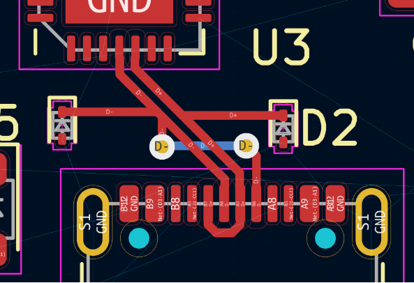
- Controlled Impedance Routing: High-speed signals (e.g., USB, HDMI, DDR) require controlled impedance traces to prevent reflections. This involves matching trace width, dielectric material, and layer spacing.
- Minimizing Crosstalk: To reduce interference between adjacent traces:
- Increase spacing between parallel traces.
- Use ground planes as shielding.
- Route critical signals on different layers orthogonally.
- Avoiding Sharp Angles: 90° turns can cause impedance discontinuities; instead, use 45° angles or curved traces.
1.2. Power and Ground Routing
Proper power distribution is essential for stable voltage supply and noise reduction.
- Power Plane Design: Use dedicated power and ground planes to minimize loop inductance and provide low-impedance paths.
- Decoupling Capacitors: Place decoupling capacitors near IC power pins to suppress high-frequency noise.
- Star Routing for Power Distribution: Avoid daisy-chaining power traces; instead, use a star topology to reduce voltage drops.
1.3. Thermal Management
Excessive heat can degrade component performance. Routing techniques to mitigate heat include:
- Wider Traces for High Current: Power traces carrying high current should be wider to reduce resistance and heat buildup.
- Thermal Relief Pads: Use thermal relief connections for components soldered to ground/power planes to ease soldering and heat dissipation.
- Via Placement for Heat Sinking: Multiple vias can help transfer heat from surface components to inner layers or heatsinks.
1.4. EMI and Noise Reduction
Electromagnetic interference (EMI) can disrupt circuit operation. Routing strategies to minimize EMI include:
- Proper Grounding: Ensure a solid ground plane and avoid ground loops.
- Differential Pair Routing: For high-speed signals (e.g., USB, PCIe), route differential pairs with consistent spacing and length matching.
- Shielding Sensitive Traces: Use guard traces or ground vias near high-frequency signals to contain EMI.
2. Advanced Routing echniques
2.1. High-Speed PCB Routing
High-speed designs (e.g., RF, DDR memory) require special considerations:
- Length Matching: Critical for differential pairs and clock signals to prevent skew.
- Impedance Control: Use stack-up calculators to determine trace width for target impedance (e.g., 50Ω for RF, 100Ω for USB).
- Via Optimization: Minimize via stubs and use back-drilling for high-frequency signals.
2.2. Mixed-Signal Routing
PCBs with both analog and digital circuits need careful isolation:
- Separate Ground Planes: Use split ground planes or a single ground with careful partitioning.
- Avoid Crossing Analog and Digital Traces: Route them on different layers with ground shielding.
2.3. Flexible and Rigid-Flex PCB Routing
Flexible PCBs introduce additional constraints:
- Avoid Sharp Bends: Use gradual curves to prevent cracking.
- Stiffeners for Component Support: Reinforce areas with heavy components.
3. Design for Manufacturability (DFM)
A well-routed PCB must also be manufacturable:
- Minimum Trace Width/Spacing: Follow the PCB fab house’s design rules.
- Via Size and Placement: Ensure vias are large enough for reliable plating.
- Testability Considerations: Include test points for debugging and production testing.
4. Common PCB Routing Mistakes to Avoid
- Ignoring Return Paths: High-speed signals need a clear return path through ground planes.
- Overloading Layers: Avoid routing all critical signals on a single layer.
- Neglecting Thermal Relief: Poor heat dissipation can lead to solder joint failures.
- Inadequate Clearance: Ensure sufficient spacing between high-voltage traces.

5. Conclusion
Effective PCB routing requires balancing electrical performance, thermal management, and manufacturability. By adhering to fundamental principles such as controlled impedance, proper grounding, and EMI reduction, designers can create reliable and high-performance PCBs. Advanced techniques like high-speed routing and mixed-signal isolation further enhance functionality. Always validate designs through simulation and collaborate with manufacturers to ensure compliance with fabrication constraints.
By mastering these PCB routing principles, engineers can optimize their designs for efficiency, reliability, and scalability in modern electronics.