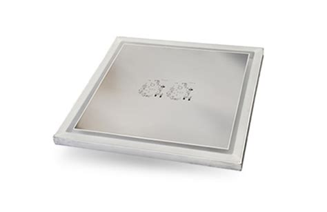
PCB Stencil Techniques for Enhanced Assembly Precision
Key Takeaways
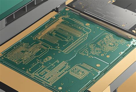
Effective PCB assembly processes rely on precision-engineered stencils to ensure consistent solder paste deposition. Modern pcba workflows increasingly adopt laser-cut stencils, which achieve ±10µm accuracy for fine-pitch components, reducing bridging and insufficient solder risks. Critical to success is aperture optimization—tailoring opening geometries to balance paste release and component footprint requirements. Electropolished surfaces further enhance transfer efficiency, particularly for micro-BGA and QFN packages.
Alignment strategies, such as fiducial marker calibration and tension-controlled frames, maintain positional accuracy during high-speed SMT placement. Material choices, including stainless steel versus hybrid nickel alloys, directly impact durability and thermal stability across repeated reflow cycles. Proactive stencil cleaning protocols—combining vacuum, chemical, and ultrasonic methods—prevent clogging and residue buildup, crucial for high-volume production.
By integrating these methods, manufacturers achieve micron-level consistency in pcb assembly, lowering defect rates by up to 40% while improving first-pass yields. This systematic approach to stencil design and maintenance ensures reliable performance across prototyping and mass-scale pcba operations.
Laser-Cut Stencil Techniques for PCB Precision
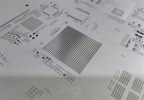
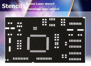
Modern PCB assembly workflows rely heavily on laser-cut stencils to achieve the micron-level accuracy required for high-density circuits. Unlike traditional chemical etching, fiber laser systems produce aperture walls with ±5µm dimensional consistency, critical for controlling solder paste volume in PCBA processes involving 01005 components or micro-BGA packages. The absence of tool wear in laser cutting ensures uniform aperture geometries across the stencil, directly impacting stencil release efficiency and minimizing solder balling defects.
Key parameters influencing laser-cut stencil performance include:
| Factor | Optimal Range | Impact on Performance |
|---|---|---|
| Material Thickness | 80-150µm | Balances paste release and durability |
| Aperture Ratio | ≥1.5 (Area) | Prevents clogging in fine-pitch designs |
| Wall Smoothness | Ra ≤0.8µm | Enhances paste transfer consistency |
For mixed-technology boards, step-down stencils created through multi-level laser ablation enable varying paste heights across the PCB. This technique proves invaluable when combining standard SMDs with large passive components in a single PCBA cycle. Proper laser parameter calibration—particularly pulse frequency (20-80kHz) and beam overlap (70-90%)—ensures clean aperture edges while maintaining stainless steel foil integrity.
Advanced manufacturers now integrate real-time vision systems with laser cutters to compensate for material warping, achieving <25µm alignment accuracy relative to panel fiducials. This precision directly translates to fewer reflow defects in high-speed PCB assembly lines, particularly when processing ultra-thin substrates common in wearable electronics.
Transitioning to laser-cut stencils requires balancing upfront costs against long-term yield improvements, but the technology remains indispensable for prototyping and mass production of HDI boards demanding ±0.3% solder volume tolerances.
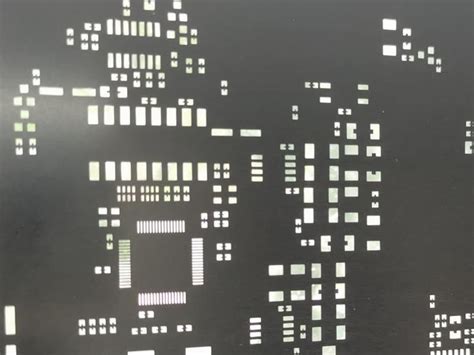
Optimizing Aperture Designs for Solder Control
Effective PCB assembly relies on precise solder paste deposition, where aperture geometry directly impacts pcba quality. Modern designs prioritize aspect ratios (aperture width-to-thickness) between 1.5:1 and 1.8:1 to ensure consistent paste release while minimizing voids or bridging. For fine-pitch components, laser-cut apertures with trapezoidal walls enhance transfer efficiency by up to 15% compared to rectangular openings, particularly for pitches below 0.4mm.
Material compatibility further refines aperture performance. Electropolished stainless steel stencils, paired with nanocoating technologies, reduce surface adhesion by 30%, enabling cleaner separation during high-speed pcb assembly processes. When optimizing for mixed-component boards, step stencils with varying thickness zones balance solder volume requirements—thinner sections for 0201 resistors, thicker regions for QFPs or BGAs.
Advanced simulation tools now model paste behavior across aperture arrays, predicting shear rates and pressure gradients to avoid solder starvation in dense layouts. Empirical validation remains critical: post-print inspections using 3D SPI (Solder Paste Inspection) systems correlate aperture adjustments with ±10μm deposition accuracy. For pcba lines handling lead-free pastes, radiused aperture corners prove essential to prevent clogging, especially after repeated cleaning cycles.
As alignment strategies evolve, aperture optimization continues to serve as the foundation for defect-free pcb assembly, bridging design intent with manufacturable outcomes.
Advanced Alignment Strategies in SMT Assembly
Precision alignment in PCB assembly relies on integrating advanced optical systems with process-controlled methodologies. Modern vision alignment systems achieve sub-10μm accuracy by analyzing PCBA fiducial markers through high-resolution cameras, compensating for board warpage or thermal drift. For multi-panel designs, step-and-repeat alignment ensures consistent registration across large batches, while 3D SPI (Solder Paste Inspection) tools validate stencil-to-board positioning in real time.
Tip: For mixed-technology boards, use dual-location fiducials — one set for the stencil and another for component placement — to mitigate alignment errors caused by material expansion.
Critical to success is selecting stencils with laser-etched alignment marks that match the PCB assembly’s copper layer geometry. Nickel-alloy stencils, favored for their low thermal expansion coefficient, maintain dimensional stability even during high-temperature reflow cycles. Additionally, dynamic squeegee pressure control adapts to uneven board surfaces, preventing solder paste smearing while ensuring uniform deposition.
To address fine-pitch components (≤0.4mm), employ micro-aperture stencils with electroformed walls, which improve paste release consistency. Pairing these with vacuum-assisted board holders reduces vibration-induced misalignment during printing. For high-density PCBA projects, automated systems leveraging AI-driven error correction can predict and adjust for positional deviations, cutting defect rates by up to 40%.
Regular calibration of alignment hardware, combined with ISO-certified cleaning protocols, sustains micron-level accuracy across production runs. This systematic approach minimizes rework and elevates first-pass yield in complex PCB assembly workflows.
Material Selection for High-Yield PCB Stencils
The performance of PCB assembly processes hinges significantly on stencil material properties, which directly influence solder paste transfer efficiency and defect rates. Stainless steel remains the industry standard for PCBA applications due to its durability, chemical resistance, and ability to maintain tight tolerances during laser cutting. For high-density designs requiring apertures below 100µm, nickel alloys offer enhanced rigidity to prevent deformation under repeated printing cycles.
Material thickness plays a critical role in balancing paste volume control and stencil longevity. While 100–150µm foils suit most surface-mount devices, thinner 50–70µm variants improve resolution for micro-BGA or 01005 components. Engineers must also consider thermal expansion coefficients when selecting substrates, as mismatched rates between stencils and PCBs during reflow can cause alignment drift.
Emerging hybrid materials, such as polyimide-coated stainless steel, combine flexibility with abrasion resistance, particularly useful for mixed-technology boards involving both PCB assembly and through-hole components. For ultra-high-yield scenarios, electropolished finishes reduce solder adhesion by achieving surface roughness values below 0.3µm Ra, simplifying cleaning protocols while maintaining paste release rates above 85%. These material innovations enable consistent solder deposition across extended production runs, directly supporting defect reduction goals outlined in earlier process optimization stages.
Effective Stencil Cleaning to Minimize Defects
Maintaining pristine PCB assembly stencils is critical for ensuring consistent solder paste deposition and reducing defects such as bridging, insufficient joints, or component misalignment. Residual solder paste, flux, or debris in apertures can compromise print quality, particularly in high-density PCBA designs where micron-level precision is essential. Automated cleaning systems utilizing ultrasonic agitation or vacuum-based solvent sprays have become industry standards, effectively removing particulate matter without damaging delicate laser-cut apertures. For PCB assembly lines handling lead-free pastes, which tend to leave harder residues, specialized cleaning solutions with pH-neutral chemistries prevent material degradation while ensuring compliance with environmental regulations.
Frequency of cleaning cycles should align with production demands—prototyping environments may require manual wipe-downs after 5-10 prints, while high-volume PCBA manufacturers often integrate inline cleaning modules that operate between consecutive prints. Implementing real-time inspection protocols using AOI (Automated Optical Inspection) systems helps detect early signs of aperture clogging or stencil warping, enabling proactive maintenance. Additionally, selecting stencil materials with anti-stick coatings, such as nano-coated stainless steel, reduces paste adhesion and extends cleaning intervals. By combining rigorous cleaning practices with material science advancements, manufacturers can achieve defect rates below 500 ppm (parts per million) while maintaining throughput in complex PCB assembly workflows. This approach directly supports the broader objective of optimizing SMT yields through precision stencil management.
Improving SMT Yields Through Stencil Optimization
Optimizing stencil designs plays a pivotal role in maximizing SMT assembly efficiency and reducing defects in PCBA manufacturing. By refining aperture geometry and thickness-to-width ratios, engineers can achieve precise solder paste deposition, directly influencing placement accuracy and joint reliability. For high-density PCB assembly, laser-cut stencils with ±10μm tolerance ensure consistent paste volume, particularly for components like 0201 resistors or 0.4mm-pitch BGAs.
Advanced step stencils and hybrid designs enable selective paste application, balancing requirements for fine-pitch ICs and large passive components within a single PCBA workflow. Real-time squeegee pressure adjustments and automated alignment systems further enhance stencil-to-PCB registration, minimizing bridging or insufficient solder. Post-printing inspection tools, such as 3D SPI, validate paste height uniformity, flagging deviations before reflow.
Material selection remains critical: stainless steel stencils with nano-coatings improve stencil release efficiency by 15–20%, while polymer-based options suit low-volume prototyping. Integrating cleaning-in-place protocols between prints reduces clogging risks, maintaining aperture integrity over 50,000+ cycles. By aligning stencil parameters with IPC-7525 standards, manufacturers systematically elevate first-pass yields, ensuring repeatable precision across mixed-technology PCB assembly lines.
Achieving Micron-Level Accuracy in PCB Assembly
Modern PCB assembly processes demand precision measured in microns to meet the escalating complexity of electronic designs. Achieving this level of accuracy begins with laser-cut stencils, which provide ±5µm dimensional consistency for solder paste deposition. Advanced aperture geometry optimization accounts for component pitch variations, using trapezoidal or stepped openings to regulate paste volume and prevent bridging or insufficient solder defects. For PCBA applications requiring fine-pitch components (≤0.4mm), electropolished stencil surfaces reduce friction, ensuring cleaner paste release.
Alignment accuracy hinges on vision-assisted fiducial systems that compensate for substrate warpage, achieving <25µm registration errors. High-end SMT assembly lines integrate real-time laser scanners to verify stencil-to-board positioning, while dynamic squeegee pressure control adapts to varying aperture densities. Material selection further influences precision: stainless steel stencils maintain rigidity for repeatable prints, while nano-coated nickel alloys resist wear in high-volume production.
To sustain micron-level performance, rigorous stencil cleaning protocols are critical. Automated vacuum-based systems remove residual paste without damaging delicate apertures, preserving print integrity across 50,000+ cycles. By harmonizing these elements, manufacturers achieve sub-20µm solder paste placement accuracy, directly enhancing PCBA reliability in aerospace, medical, and 5G applications.
Defect Reduction with Precision Stencil Methods
Precision stencil methods play a critical role in minimizing defects during PCB assembly, directly impacting the reliability of PCBA outcomes. Modern laser-cut stencils achieve tolerances as tight as ±5µm, ensuring consistent solder paste deposition while reducing risks of bridging or insufficient solder volume. By optimizing aperture geometry—such as trapezoidal walls or nano-coated surfaces—manufacturers improve paste release efficiency, particularly for fine-pitch components like 0201 resistors or 0.4mm-pitch BGAs.
Advanced alignment systems, including vision-assisted fiducial markers and dynamic tension control frameworks, maintain ±25µm registration accuracy across high-density boards. This precision prevents misalignment-induced defects such as tombstoning or skewed component placement. For high-volume PCBA production, selecting stencils with durable electropolished stainless steel or hybrid nickel alloys extends service life while resisting wear-induced inconsistencies.
Equally critical are cleaning protocols that prevent paste residue buildup. Automated wiping cycles with solvent-free cleaners reduce solder ball formation by 40–60% compared to manual methods. Combining these strategies with real-time process monitoring enables defect rates below 50ppm in controlled environments, making precision stencil techniques indispensable for achieving Six Sigma-level quality in modern PCB assembly workflows.
Conclusion
The pursuit of precision in PCB assembly relies on harmonizing advanced stencil methodologies with rigorous process controls. By integrating laser-cut techniques and aperture optimization, manufacturers achieve micron-level accuracy in solder paste deposition, directly enhancing PCBA reliability. Strategic alignment protocols, coupled with material innovations like nano-coated stainless steel, further reduce bridging and skewing risks. Equally critical are systematic cleaning cycles that preserve stencil integrity across production runs, preventing residue accumulation that could compromise solder joint quality. These refinements collectively address defects common in high-density designs, such as tombstoning or insufficient solder volume, while supporting repeatable outcomes in both prototyping and volume manufacturing. As component miniaturization continues, the role of optimized stencils in SMT assembly becomes increasingly pivotal—transforming theoretical precision into measurable yield improvements. By prioritizing data-driven adjustments and material science advancements, engineers can maintain alignment with evolving industry standards for PCB assembly performance.
FAQs
What role do stencils play in achieving precision in pcb assembly?
PCB stencils ensure accurate solder paste deposition by controlling volume and placement. Advanced laser-cut designs enable micron-level accuracy, critical for high-density PCBA boards. Proper aperture optimization reduces bridging and voiding, directly impacting first-pass yield rates.
How do alignment strategies affect pcb assembly quality?
Misalignment during SMT assembly causes skewed solder deposits, leading to tombstoning or opens. Modern systems use vision-assisted frameworks with fiducial markers and optical recognition to maintain ±25µm registration. Automated calibration further enhances repeatability across production batches.
Which materials are optimal for high-performance stencils?
Electropolished stainless steel remains standard for durability and fine-pitch compatibility. For ultra-fine features (<0.3mm pitch), nickel alloys or hybrid materials improve paste release. Material choice directly impacts cleaning protocols—smoother surfaces resist clogging and simplify maintenance.
What cleaning methods minimize defects in pcb assembly?
Combining mechanical wiping with vacuum extraction removes residual paste without damaging apertures. For lead-free pastes, semi-aqueous cleaners prevent oxidation. Daily inspections and nano-coating treatments extend stencil lifespan while reducing downtime.
Can stencil design improve SMT assembly yields for mixed-technology boards?
Yes. Step stencils with multiple thicknesses accommodate both 01005 components and large connectors. Dynamic aperture shaping accounts for paste slump, ensuring consistent volume across varied pad geometries. This approach reduces rework in PCBA prototypes and mass production.
Optimize Your Next Project with Expert Guidance
For tailored solutions in pcb assembly and stencil design, please click here to consult our engineering team. Leverage industry-leading techniques to elevate your PCBA quality and efficiency.


