PCB Stick-On Stencils: A Comprehensive Guide to Efficient Solder Paste Application
Introduction to PCB Stick-On Stencils
Printed Circuit Board (PCB) manufacturing has evolved significantly over the past few decades, with surface mount technology (SMT) becoming the dominant method for component assembly. At the heart of this process lies the critical step of solder paste application, where PCB stencils play an indispensable role. Among the various types of stencils available, stick-on stencils have emerged as a popular choice for many electronics manufacturers, particularly for prototyping and low-to-medium volume production.
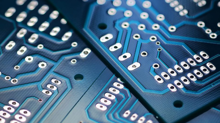
PCB stick-on stencils, as the name suggests, are thin metal sheets with precisely cut apertures that adhere directly to the PCB surface during the solder paste printing process. These stencils offer a convenient, cost-effective solution for applying solder paste to PCB pads with high accuracy and repeatability. Unlike framed stencils that require tensioning systems, stick-on stencils utilize adhesive backing or other temporary bonding methods to maintain proper alignment with the board.
The importance of solder paste stenciling in PCB assembly cannot be overstated. This process determines the volume, shape, and placement accuracy of solder paste deposits, which directly affects the quality of solder joints during reflow. Proper stenciling minimizes defects such as bridging, insufficient solder, or component misalignment—issues that can lead to costly rework or product failures.
This comprehensive guide will explore the various aspects of PCB stick-on stencils, including their materials, manufacturing processes, application techniques, advantages, limitations, and best practices for optimal performance. Whether you’re an electronics engineer, PCB designer, or manufacturing professional, understanding these stencils will help you make informed decisions for your assembly processes.

Materials and Construction of Stick-On Stencils
Stencil Materials
The performance and durability of PCB stick-on stencils largely depend on the materials used in their construction. The most common materials include:
- Stainless Steel: The industry standard for high-quality stencils, typically 304 or 304L grade stainless steel. Offers excellent durability, chemical resistance, and precise aperture walls. Common thicknesses range from 0.1mm to 0.2mm (4-8 mils) for most SMT applications.
- Nickel: Sometimes used for specialized applications requiring extra durability or chemical resistance. Nickel stencils can withstand more cleaning cycles than stainless steel but are more expensive.
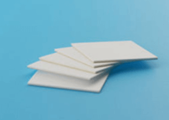
- Polyimide (Kapton): A flexible polymer material used for ultra-thin stencils or unusual applications. Less durable than metal but useful for certain prototyping situations.
The material choice affects stencil life, paste release characteristics, and cleaning requirements. Stainless steel remains the preferred choice for most professional applications due to its optimal balance of performance and cost.
Adhesive Systems
The “stick-on” feature of these stencils relies on various adhesive technologies:
- Pressure-Sensitive Adhesives (PSA): The most common type, these adhesives bond when light pressure is applied. They allow for multiple placements and removals while maintaining sufficient tack.
- Reusable Adhesive Films: Special films that can be reapplied multiple times without losing their adhesive properties. These often come as separate sheets that are applied to the stencil’s perimeter.
- Temporary Bonding Sprays: Some systems use spray adhesives applied just before stencil use. These offer adjustable tack but require more careful handling.
The adhesive must be strong enough to hold the stencil firmly in place during printing but not so aggressive that it damages the PCB or leaves residue upon removal. Many modern adhesives are designed to be residue-free or leave only minimal deposits that are easily cleaned.
Stencil Thickness Considerations
Stencil thickness is a critical parameter that directly affects solder paste volume:
- Standard Thickness: 0.1-0.15mm (4-6 mils) for typical SMT components
- Fine-Pitch Applications: 0.075-0.1mm (3-4 mils) for components with pitches below 0.5mm
- Large Components: 0.15-0.2mm (6-8 mils) for components requiring more solder paste like QFPs or BGAs
The thickness must be selected based on the smallest component pitch in the design and the required solder joint characteristics. Many stick-on stencils use uniform thickness, but some advanced versions incorporate step-down regions for mixed-technology boards.
Manufacturing Processes for Stick-On Stencils
Laser Cutting Technology
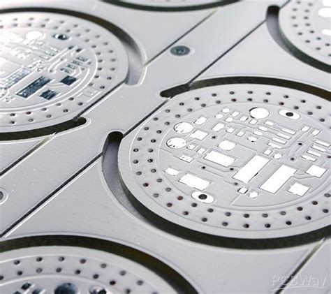
Most high-quality PCB stick-on stencils are manufactured using laser cutting technology:
- Fiber Laser Cutting: The most common method, offering excellent precision (up to ±10μm) and smooth aperture walls. Fiber lasers can cut stainless steel up to 0.2mm thick with minimal heat-affected zones.
- Chemical Etching: An alternative process where the stencil pattern is etched using photochemical methods. Less precise than laser cutting but can be more cost-effective for very simple designs.
- Electroforming: A specialized process that builds up nickel stencils through electrodeposition. Creates very smooth aperture walls but is more expensive and less common for stick-on stencils.
Laser-cut stencils offer several advantages:
- Excellent positional accuracy matching the PCB design
- Smooth aperture walls that promote good paste release
- Ability to create complex aperture shapes (including stepped stencils)
- Fast turnaround times (often same-day service)
Design and Fabrication Process
The typical stick-on stencil manufacturing process involves:
- File Preparation: The PCB Gerber files (usually the paste layer) are processed and optimized for stencil production. This may include adjustments for aperture size compensation or special shapes.
- Laser Programming: The cutting path is programmed into the laser system based on the processed design files.
- Material Preparation: The stainless steel sheet is cleaned and, if needed, coated with adhesive on one side.
- Laser Cutting: The pattern is precisely cut into the metal sheet using the laser system.
- Cleaning and Inspection: The finished stencil undergoes cleaning to remove any debris or slag from cutting, followed by rigorous quality inspection.
- Packaging: The stencil is carefully packaged to prevent damage during shipping, often with protective films on both sides.
Advanced manufacturers may use optical inspection systems to verify aperture sizes and positions against the original design, ensuring high accuracy before shipment.
Advantages of Stick-On Stencils
Cost-Effectiveness
One of the primary benefits of stick-on stencils is their cost advantage:
- Lower Initial Cost: Typically 30-50% less expensive than framed stencils
- No Frame Expense: Eliminates the cost of aluminum frames and tensioning mesh
- Reduced Shipping Costs: Lighter and more compact than framed stencils
- Inventory Savings: Easier to store multiple stencils for different designs
This makes stick-on stencils particularly attractive for:
- Prototyping and R&D
- Low-volume production
- Educational purposes
- Hobbyist projects
Space Efficiency and Storage
The compact nature of stick-on stencils offers several logistical advantages:
- Minimal Storage Requirements: Can be stored flat in folders or envelopes
- Easy Organization: Multiple stencils can be kept for various designs without consuming much space
- Portability: Easy to transport between locations or worksites
For facilities with limited space or those managing many different PCB designs, these space-saving characteristics can be significant.
Setup Simplicity
Stick-on stencils simplify the solder paste printing process:
- No Special Equipment Needed: Can be used without expensive stencil printers
- Quick Changeovers: Switching between different PCB designs is faster
- Manual Printing Friendly: Well-suited for hand-printing operations
This simplicity makes them ideal for:
- Small batch production
- Engineering verification
- Field service repairs
- Educational environments
Flexibility and Adaptability
The stick-on format allows for creative solutions:
- Partial Stencils: Can be made for specific board sections only
- Multi-Board Stencils: Single stencil can cover multiple small PCBs
- Rework Stencils: Small stencils for touch-up or repair work
- Experimental Designs: Easy to modify or create custom stencils
This flexibility supports rapid iteration and design changes during development cycles.
Limitations and Challenges
Alignment Difficulties
One of the main challenges with stick-on stencils is achieving and maintaining proper alignment:
- Manual Alignment: Requires careful visual alignment with PCB pads
- Registration Marks: May not have fiducials for optical alignment systems
- Shifting Risk: Possible movement during printing, especially with manual squeegee use
Solutions to improve alignment include:
- Using alignment pins or corner adhesives
- Incorporating clear sections for visual verification
- Creating custom alignment jigs
Durability Concerns
Compared to framed stencils, stick-on versions have some durability limitations:
- Adhesive Wear: The sticky surface may lose effectiveness after multiple uses
- Thinner Materials: More prone to bending or creasing with handling
- Cleaning Sensitivity: Aggressive cleaning can damage adhesive properties
Proper handling and storage can extend stencil life significantly.
Paste Release Characteristics
The nature of stick-on stencils can sometimes affect paste release:
- No Tension: Lack of frame tension may cause stencil to lift unevenly
- Adhesive Interference: Paste may occasionally stick to adhesive areas
- Flex Issues: Thin materials may flex during squeegee motion
These issues can be mitigated through:
- Proper squeegee technique
- Optimal adhesive placement (away from apertures)
- Appropriate stencil thickness selection
Best Practices for Using Stick-On Stencils
Proper Application Techniques
To achieve optimal results with stick-on stencils:
- Surface Preparation:
- Ensure PCB surface is clean and free of debris
- Remove any oxidation that might affect adhesion
- Stencil Alignment:
- Use magnification for precise alignment
- Align to at least two corners before full adhesion
- Consider using alignment pins for critical designs
- Adhesion Process:
- Apply stencil starting from one edge to avoid air bubbles
- Use firm, even pressure to ensure complete bonding
- Pay special attention to areas with fine-pitch components
- Printing Technique:
- Use consistent squeegee angle (typically 45-60°)
- Maintain even pressure during stroke
- Consider multiple passes for better paste filling
Cleaning and Maintenance
Proper care extends stencil life and maintains print quality:
- Immediate Cleaning:
- Remove solder paste promptly after printing
- Use appropriate cleaning solvents (isopropyl alcohol common)
- Avoid abrasive materials that could damage apertures
- Adhesive Maintenance:
- Clean adhesive areas gently to preserve tack
- Store with protective liner when not in use
- Refresh adhesive with specialized sprays if needed
- Inspection Routine:
- Regularly check for clogged apertures
- Verify adhesive effectiveness at edges
- Inspect for any physical damage or deformation
Storage Recommendations
Proper storage preserves stencil quality:
- Flat Storage: Keep stencils flat in protective sleeves or folders
- Environment Control: Store in clean, dry conditions
- Separation: Use protective sheets between stacked stencils
- Labeling: Clearly mark stencils with PCB design and revision
Advanced Applications and Variations
Multi-Layer Stencils
Some advanced stick-on stencils incorporate multiple layers:
- Stepped Stencils: Different thickness areas for mixed components
- Multi-Level Stencils: For complex PCB architectures
- Hybrid Designs: Combining stencil and dispensing functions
Specialized Adhesive Patterns
Innovative adhesive configurations address specific needs:
- Perimeter-Only Adhesion: Minimizes contact with PCB surface
- Patterned Adhesives: Strategic placement for optimal hold
- Adjustable Tack Systems: Allow for adhesion strength control
Integrated Alignment Systems
Some stick-on stencils incorporate alignment aids:
- Transparent Sections: For visual alignment verification
- Mechanical Guides: Built-in alignment features
- Magnetic Assist: Combining adhesive with magnetic alignment
Future Trends in Stick-On Stencil Technology
The stick-on stencil market continues to evolve with several emerging trends:
- Smart Adhesives: Developing adhesives with precisely controlled tack and clean release properties
- Advanced Materials: Exploring new metal alloys and composites for improved performance
- Automation Integration: Designing stick-on stencils compatible with semi-automated systems
- Sustainability Focus: Creating recyclable stencils and eco-friendly adhesive systems
- Digital Integration: Incorporating QR codes or RFID tags for stencil identification and tracking
As PCB technology advances with finer pitches and more complex components, stick-on stencil technology will continue to adapt to meet these challenges while maintaining its cost and convenience advantages.
Conclusion
PCB stick-on stencils represent a versatile and cost-effective solution for solder paste application across a wide range of electronics manufacturing scenarios. From prototyping and low-volume production to educational use and field service, these stencils offer significant advantages in terms of cost, space efficiency, and operational flexibility.
While they may not replace framed stencils in high-volume automated production environments, stick-on stencils fill an important niche in the electronics manufacturing ecosystem. Their continued development and refinement ensure they will remain a valuable tool for engineers and manufacturers seeking quality solder paste deposition without the overhead of traditional stencil systems.
By understanding the materials, construction, proper usage techniques, and limitations of stick-on stencils, electronics professionals can make informed decisions about when and how to implement this practical technology in their PCB assembly processes. With proper selection, application, and maintenance, stick-on stencils can deliver excellent results that rival more expensive alternatives while providing unmatched convenience and flexibility.