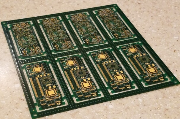
Pcb sub assembly and design
Importance Of Quality Control In PCB Sub Assembly
In the realm of electronics manufacturing, the significance of quality control in PCB sub-assembly cannot be overstated. Printed Circuit Boards (PCBs) serve as the backbone of virtually all electronic devices, from simple household gadgets to complex industrial machinery. Ensuring the reliability and functionality of these devices hinges on the meticulous assembly and inspection of PCBs. Consequently, quality control in PCB sub-assembly emerges as a critical factor that can determine the success or failure of the final product.
To begin with, quality control in PCB sub-assembly involves a series of systematic procedures designed to detect and rectify defects at various stages of the manufacturing process.
This proactive approach is essential because even minor flaws in a PCB can lead to significant malfunctions, potentially causing device failures or, in severe cases, safety hazards. By implementing rigorous quality control measures, manufacturers can identify and address issues early, thereby preventing costly rework or recalls down the line.
Moreover, the complexity of modern electronic devices necessitates a high degree of precision in PCB sub-assembly.
Components are becoming increasingly miniaturized, and the density of circuits on a single board is continually rising. This trend amplifies the potential for errors during assembly, making quality control even more crucial. Advanced inspection techniques, such as Automated Optical Inspection (AOI) and X-ray inspection, play a pivotal role in maintaining the integrity of these intricate assemblies. These technologies enable the detection of minute defects that might be invisible to the naked eye, ensuring that each PCB meets stringent quality standards.
In addition to detecting defects, quality control in PCB sub-assembly also encompasses the verification of component placement and soldering quality.
Accurate component placement is vital for the proper functioning of the PCB, as even a slight misalignment can disrupt the entire circuit. Similarly, the quality of solder joints is paramount, as poor soldering can lead to weak connections and intermittent failures. Through techniques like solder paste inspection and in-circuit testing, manufacturers can ensure that components are correctly positioned and securely soldered, thereby enhancing the overall reliability of the PCB.
Furthermore, the implementation of quality control in PCB sub-assembly extends beyond the technical aspects of inspection and testing.
It also involves adherence to industry standards and regulatory requirements. Compliance with standards such as IPC-A-610, which outlines the acceptability criteria for electronic assemblies, is essential for maintaining consistency and reliability across different production batches. By adhering to these standards, manufacturers can assure customers of the quality and dependability of their products, thereby fostering trust and confidence in their brand.
Another critical aspect of quality control in PCB sub-assembly is the continuous improvement of processes.
By analyzing data from quality control inspections and identifying recurring issues, manufacturers can implement corrective actions and refine their assembly processes. This iterative approach not only enhances the quality of the current production but also contributes to the long-term improvement of manufacturing practices. Consequently, manufacturers can achieve higher yields, reduce waste, and optimize production efficiency.
In conclusion, the importance of quality control in PCB sub-assembly is multifaceted, encompassing defect detection, component verification, compliance with standards, and continuous process improvement. As electronic devices become more sophisticated and integral to our daily lives, the need for reliable and high-quality PCBs becomes increasingly critical. Through diligent quality control practices, manufacturers can ensure the performance, safety, and longevity of their products, ultimately contributing to the advancement of technology and the betterment of society..
Key Steps In The PCB Sub Assembly Process
Printed Circuit Board (PCB) sub-assembly is a critical phase in the electronics manufacturing process, involving the integration of various electronic components onto a PCB to create functional modules. This process is essential for ensuring the reliability and performance of electronic devices. To understand the key steps in the PCB sub-assembly process, it is important to delve into the intricacies of each stage, from initial preparation to final inspection.
The process begins with the preparation of the PCB itself.
This involves cleaning the board to remove any contaminants that could interfere with the soldering process. The board is then inspected for any defects or irregularities that could affect its performance. Once the PCB is deemed ready, the next step is the application of solder paste. Solder paste is a mixture of tiny solder balls and flux, which helps in the soldering process by cleaning and preparing the surfaces to be joined. The paste is applied to the board using a stencil, ensuring that it is deposited only on the pads where components will be placed.
Following the application of solder paste, the placement of components is the next critical step.
This is typically done using automated pick-and-place machines, which accurately position components onto the PCB based on a pre-programmed layout. These machines are capable of placing a wide variety of components, from tiny resistors and capacitors to larger integrated circuits. The precision of this step is crucial, as any misalignment can lead to defects in the final product.
Once the components are in place, the assembly moves to the soldering phase.
There are several methods for soldering, with reflow soldering being the most common for surface-mount technology (SMT) components. In reflow soldering, the PCB is passed through a reflow oven, where it is gradually heated to melt the solder paste, creating a strong bond between the components and the board. For through-hole components, wave soldering is often used, where the PCB is passed over a wave of molten solder, allowing the solder to flow into the holes and create secure connections.
After soldering, the PCB undergoes a thorough cleaning process to remove any residual flux and other contaminants.
This is typically done using specialized cleaning agents and equipment. The cleanliness of the board is vital for preventing corrosion and ensuring long-term reliability.
The next step is inspection and testing. Automated optical inspection (AOI) systems are commonly used to check for soldering defects, component misalignment, and other issues. These systems use high-resolution cameras and advanced algorithms to detect even the smallest defects. In addition to AOI, X-ray inspection may be employed to examine solder joints that are not visible to the naked eye, such as those beneath ball grid array (BGA) components.
Functional testing is also a crucial part of the inspection process. This involves applying power to the PCB and running a series of tests to ensure that it operates as intended. Any defects identified during this stage are addressed through rework, where the faulty components are replaced or repaired.
Finally, the assembled PCB undergoes a final inspection to ensure that it meets all quality standards and specifications
. This includes a visual inspection, as well as additional functional tests if necessary. Once the PCB passes this final inspection, it is ready for integration into the final product.
In conclusion, the PCB sub-assembly process is a complex and meticulous procedure that requires careful attention to detail at every stage. From initial preparation and component placement to soldering, cleaning, and inspection, each step is crucial for ensuring the reliability and performance of the final product. By understanding these key steps, manufacturers can produce high-quality PCBs that meet the demanding requirements of modern electronic devices.
Common Challenges In PCB Sub Assembly And How To Overcome Them
Printed Circuit Board (PCB) sub-assembly is a critical phase in the electronics manufacturing process, involving the integration of various electronic components onto a PCB. Despite its importance, this stage is fraught with numerous challenges that can impact the overall quality and functionality of the final product. Understanding these common challenges and implementing effective strategies to overcome them is essential for ensuring a successful PCB sub-assembly process.
One of the primary challenges in PCB sub-assembly is component placement accuracy.
The precision with which components are placed on the PCB is crucial, as even minor misalignments can lead to functional failures or reduced performance. To address this issue, manufacturers often employ automated pick-and-place machines, which offer high precision and repeatability. Additionally, implementing rigorous quality control measures, such as optical inspection systems, can help detect and correct placement errors early in the process.
Another significant challenge is soldering defects, which can manifest as solder bridges, cold joints, or insufficient solder coverage.
These defects can compromise the electrical connectivity and reliability of the PCB. To mitigate soldering issues, it is essential to optimize the soldering process parameters, including temperature profiles and solder paste composition. Utilizing advanced soldering techniques, such as reflow soldering and wave soldering, can also enhance the quality of solder joints. Furthermore, regular maintenance and calibration of soldering equipment are vital to ensure consistent performance.
Thermal management is another critical aspect that poses challenges during PCB sub-assembly.
Electronic components generate heat during operation, and inadequate thermal management can lead to overheating, component failure, and reduced lifespan of the PCB. To overcome thermal management issues, designers must carefully consider the placement of heat-sensitive components and incorporate thermal vias, heat sinks, and thermal pads into the PCB design. Additionally, using materials with high thermal conductivity and implementing proper airflow management within the enclosure can help dissipate heat effectively.
Component compatibility and availability also present significant challenges in PCB sub-assembly.
The rapid pace of technological advancements often leads to component obsolescence, making it difficult to source compatible parts. To address this issue, manufacturers should establish strong relationships with reliable suppliers and maintain an updated database of alternative components. Additionally, designing PCBs with flexibility in mind, such as using standardized footprints and pin configurations, can facilitate the substitution of components without major redesigns.
Electromagnetic interference (EMI) is another challenge that can affect the performance of PCBs.
EMI can cause signal degradation, data corruption, and even complete system failure. To mitigate EMI issues, designers should implement proper grounding and shielding techniques, such as using ground planes, ferrite beads, and EMI shields. Additionally, careful routing of high-frequency signals and maintaining adequate spacing between traces can help minimize EMI.
Finally, ensuring the reliability and durability of PCBs is a critical challenge in sub-assembly.
Environmental factors, such as humidity, temperature fluctuations, and mechanical stress, can impact the long-term performance of PCBs. To enhance reliability, manufacturers should conduct thorough testing, including thermal cycling, vibration testing, and humidity exposure tests. Implementing conformal coatings and encapsulation techniques can also protect PCBs from environmental damage.
In conclusion, PCB sub-assembly is a complex process that involves numerous challenges, ranging from component placement accuracy to thermal management and EMI mitigation. By employing advanced technologies, optimizing process parameters, and implementing robust quality control measures, manufacturers can effectively overcome these challenges and ensure the production of high-quality, reliable PCBs.
Innovations In PCB Sub Assembly Technology
Printed Circuit Board (PCB) sub-assembly technology has undergone significant advancements in recent years, driven by the increasing complexity and miniaturization of electronic devices. These innovations have not only enhanced the performance and reliability of electronic products but have also streamlined manufacturing processes, reducing costs and improving efficiency.
One of the most notable advancements in PCB sub-assembly technology is the development of surface mount technology (SMT).
SMT has revolutionized the way components are mounted onto PCBs, allowing for smaller, lighter, and more complex assemblies. Unlike traditional through-hole technology, which requires drilling holes into the PCB for component leads, SMT components are placed directly onto the surface of the board. This method not only saves space but also enables higher component density, leading to more compact and efficient designs.
In addition to SMT, the advent of advanced materials has played a crucial role in the evolution of PCB sub-assembly technology.
High-performance substrates, such as polyimide and ceramic, offer superior thermal and electrical properties compared to traditional FR4 materials. These advanced substrates can withstand higher temperatures and provide better signal integrity, making them ideal for high-frequency and high-power applications. Furthermore, the use of flexible and rigid-flex PCBs has expanded the possibilities for innovative product designs, particularly in wearable electronics and medical devices.
Another significant innovation in PCB sub-assembly technology is the integration of automated assembly processes.
Automation has become increasingly prevalent in PCB manufacturing, with robotic systems and advanced machinery taking over tasks that were once performed manually. Automated pick-and-place machines, for example, can accurately position thousands of components per hour, significantly reducing assembly time and minimizing the risk of human error. Additionally, automated optical inspection (AOI) systems are now commonly used to detect defects and ensure the quality of assembled PCBs. These systems use high-resolution cameras and sophisticated algorithms to inspect solder joints, component placement, and other critical aspects of the assembly process.
The rise of Industry 4.0 and the Internet of Things (IoT) has further propelled innovations in PCB sub-assembly technology.
Smart manufacturing techniques, such as real-time monitoring and data analytics, enable manufacturers to optimize production processes and improve yield rates. By collecting and analyzing data from various stages of the assembly process, manufacturers can identify potential issues early on and implement corrective actions before they escalate. This proactive approach not only enhances product quality but also reduces waste and lowers production costs.
Moreover, advancements in PCB sub-assembly technology have also led to the development of more sophisticated testing and validation methods.
In-circuit testing (ICT) and functional testing are now more comprehensive and efficient, ensuring that assembled PCBs meet stringent quality standards. These testing methods can detect a wide range of defects, from open circuits and short circuits to incorrect component values and functional failures. By thoroughly testing each PCB sub-assembly, manufacturers can guarantee the reliability and performance of their products, ultimately leading to higher customer satisfaction.
In conclusion, the continuous innovations in PCB sub-assembly technology have significantly transformed the electronics manufacturing industry. From surface mount technology and advanced materials to automated assembly processes and smart manufacturing techniques, these advancements have paved the way for more efficient, reliable, and cost-effective production of electronic devices. As technology continues to evolve, we can expect further improvements in PCB sub-assembly processes, driving the development of even more sophisticated and high-performing electronic products.


