PCB Sustainability: Breaking Through the Environmental Bottleneck
Introduction
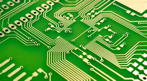
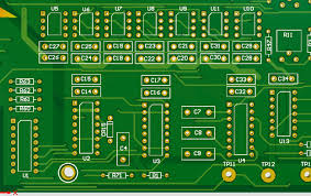
The printed circuit board (PCB) industry is a cornerstone of modern electronics, enabling the functionality of devices ranging from smartphones to industrial machinery. However, as global demand for electronics grows, so does the environmental footprint of PCB manufacturing. The industry faces significant sustainability challenges, including hazardous waste generation, high energy consumption, and reliance on non-renewable materials. To achieve long-term sustainability, the PCB sector must overcome these environmental bottlenecks through innovation, regulatory compliance, and circular economy practices.
This article explores the key environmental challenges in PCB production, examines emerging solutions, and highlights the role of stakeholders in driving sustainable transformation.
Environmental Challenges in PCB Manufacturing
1. Hazardous Materials and Waste
Traditional PCB manufacturing involves toxic chemicals, including heavy metals (lead, cadmium, mercury), brominated flame retardants (BFRs), and volatile organic compounds (VOCs). These substances pose risks to human health and ecosystems if improperly disposed of. Additionally, etching processes generate wastewater contaminated with copper and other metals, requiring costly treatment.
2. High Energy and Resource Consumption
PCB fabrication is energy-intensive, particularly in processes like lamination, plating, and soldering. The reliance on fossil fuels contributes to greenhouse gas emissions. Moreover, PCBs depend on finite resources such as copper, gold, and rare earth elements, raising concerns about long-term supply chain sustainability.
3. Limited Recycling and End-of-Life Management
Electronic waste (e-waste) is one of the fastest-growing waste streams globally, with PCBs being a major contributor. Despite containing valuable metals, PCB recycling remains inefficient due to:
- Complex material composition – Difficult separation of metals, plastics, and ceramics.
- Informal recycling practices – In developing countries, crude methods (e.g., open burning) release toxic fumes.
- Low recovery rates – Only ~20-30% of PCB materials are currently recycled effectively.
4. Regulatory and Compliance Pressures
Environmental regulations such as the EU’s Restriction of Hazardous Substances (RoHS) and Waste Electrical and Electronic Equipment (WEEE) directives impose strict limits on hazardous substances and mandate recycling. Non-compliance can result in fines and market exclusion, pushing manufacturers toward greener alternatives.
Breaking the Environmental Bottleneck: Key Strategies
1. Adoption of Green Materials
- Lead-Free and Halogen-Free PCBs – Transitioning to lead-free solders (e.g., SAC alloys) and eliminating brominated flame retardants reduces toxicity.
- Bio-Based Substrates – Research into biodegradable or plant-based PCB materials (e.g., cellulose composites) could lower environmental impact.
- Alternative Conductive Inks – Silver and copper nanoparticle inks reduce metal usage and enable additive manufacturing.
2. Energy-Efficient Manufacturing Processes
- Renewable Energy Integration – Factories powered by solar or wind energy can significantly cut carbon emissions.
- Advanced Manufacturing Techniques – Laser direct structuring (LDS) and inkjet printing minimize material waste compared to traditional etching.
- Process Optimization – AI-driven predictive maintenance and smart energy management reduce energy waste.
3. Enhanced Recycling and Circular Economy Models
- Urban Mining – Recovering precious metals from discarded PCBs through hydrometallurgical or bioleaching methods.
- Design for Disassembly (DfD) – Modular PCB designs simplify component separation for recycling.
- Extended Producer Responsibility (EPR) – Manufacturers take accountability for product lifecycle management, incentivizing eco-design.
4. Regulatory and Industry Collaboration
- Stricter Enforcement of E-Waste Laws – Governments must combat illegal e-waste dumping and support formal recycling channels.
- Industry Certifications – Standards like IPC-1401 (Sustainability for Electronics) guide eco-friendly PCB production.
- Cross-Sector Partnerships – Collaboration among OEMs, recyclers, and policymakers accelerates sustainable innovation.
Case Studies: Pioneering Sustainable PCB Initiatives
1. Apple’s Closed-Loop Supply Chain
Apple has invested in robotic disassembly (e.g., Daisy robot) to recover materials from iPhones, including gold and copper from PCBs. The company aims to eliminate mining by using 100% recycled materials.
2. European Horizon 2020 Projects
Initiatives like CircEl-Paper explore recyclable PCBs made from paper-based substrates, demonstrating feasibility in low-power applications.
3. Taiwanese PCB Manufacturers’ Green Transition
Companies like Unimicron and Compeq have adopted water-saving technologies and reduced hazardous chemical usage, aligning with global sustainability goals.
The Path Forward
While progress is being made, systemic barriers remain:
- Cost Considerations – Sustainable alternatives often require higher upfront investments.
- Technological Limitations – Some green materials lack the durability of conventional PCBs.
- Consumer Awareness – Demand for cheaper electronics often outweighs environmental concerns.
To overcome these hurdles, a multi-stakeholder approach is essential:
- Governments should incentivize green manufacturing through subsidies and tax breaks.
- Corporations must prioritize sustainability in R&D and supply chain management.
- Consumers can drive change by supporting eco-conscious brands and proper e-waste disposal.
Conclusion
The PCB industry stands at a crossroads—balancing technological advancement with environmental responsibility. By embracing green materials, energy-efficient processes, and circular economy principles, manufacturers can break through the sustainability bottleneck. The transition will require innovation, investment, and collaboration, but the payoff—a cleaner, more sustainable electronics ecosystem—is well worth the effort.
The future of PCBs lies not just in performance and miniaturization, but in sustainability. The time to act is now.