PCB Technical Guide Design Process
In PCB design, before formal wiring, there are actually a lot of steps to go through. The following is the main design process:
—-System Specifications
First, the system specifications of the electronic device must be planned. Including system functions, cost constraints, size, operating conditions, etc.
—-System Function Block Diagram
Next, the system function block diagram must be made. The relationship between the blocks must also be marked.
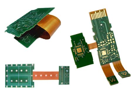
—-Segment the system into several PCBs
If the system is divided into several PCBs, it can not only be reduced in size, but also allow the system to have the ability to upgrade and exchange parts. The system function block diagram provides the basis for our division. For example, a computer can be divided into a motherboard, a display card, a sound card, a floppy disk drive, and a power supply, etc.

—-Decide on the packaging method to be used, and the size of each PCB
When the technology and number of circuits used in each PCB are determined, the next step is to determine the size of the board. If the design is too large, the packaging technology must be changed, or the division must be re-performed. When choosing technology, the quality and speed of the circuit diagram must also be taken into consideration.
—-Draw a schematic diagram of all PCBs
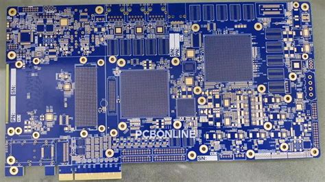
The schematic diagram should show the interconnection details between the components. All PCBs in the system must be drawn, and most of them are now designed using CAD (Computer Aided Design). The following is an example of using CircuitMakerTM design.
PCB circuit diagram
—-Simulation operation of preliminary design
In order to ensure that the designed circuit diagram can work properly, it must be simulated once using computer software. This type of software can read the design drawing and display the circuit operation in many ways. This is much more efficient than actually making a sample PCB and then measuring it manually.
—-Put the parts on the PCB
The way the parts are placed is determined by how they are connected to each other. They must be connected to the path in the most efficient way. The so-called efficient routing means that the shorter the wires and the fewer layers they pass through (this also reduces the number of guide holes), the better, but we will mention this issue again when we actually route. The following is how the bus is routed on the PCB. In order for each component to have perfect wiring, the placement is very important.
—-Testing wiring possibilities and correct operation at high speeds
Some computer software today can check whether the positions of various components can be connected correctly, or whether they can operate correctly at high speeds. This step is called arranging components, but we will not go into this in depth. If there is a problem with the circuit design, the positions of the components can be rearranged before the actual circuit is exported.

—-Exporting the circuit on the PCB
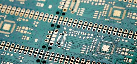
The connections in the schematic will now be made into the actual wiring. This step is usually fully automatic, but generally some parts need to be changed manually. Below is the wire template for a 2-layer board. The red and blue lines represent the component layer and the solder layer of the PCB respectively. The white text and squares represent the various markings on the screen printing surface. The red dots and circles represent drill holes and guide holes. On the far right, we can see that there are gold fingers on the soldering surface of the PCB. The final composition of this PCB is usually called a work film (Artwork).
Every design must meet a set of regulations, such as the minimum reserved space between circuits, the minimum circuit width, and other similar practical restrictions. These regulations vary according to the speed of the circuit, the strength of the transmitted signal, the circuit’s sensitivity to power consumption and noise, as well as the quality of the material and manufacturing equipment. If the current intensity increases, the thickness of the wire must also be increased. In order to reduce the cost of the PCB, while reducing the number of layers, it is also necessary to pay attention to whether these regulations are still met. If a structure with more than 2 layers is required, a power layer and a ground layer are usually used to prevent the transmitted signal on the signal layer from being affected, and can be used as a shield for the signal layer.