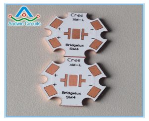
Pcb thermal pad vias
PCB thermal pad vias are typically used in electronic devices that generate a lot of heat,
such as microprocessors, power amplifiers, and voltage regulators.
The thermal pad via is used to transfer heat from the component to the ground plane of the PCB,
which helps to dissipate the heat and prevent damage to the component.
The thermal pad via is typically connected to multiple vias that are distributed across the PCB,
which helps to distribute the heat more evenly and prevent hot spots from forming.

PCB thermal pad vias are small holes drilled through the thermal pad on a printed circuit board (PCB) to allow heat to flow from the pad to the internal layers of the board.
The vias are typically filled with a conductive material,
such as copper, to provide a low thermal resistance path for heat to flow through.
The purpose of using thermal pad vias is to improve the thermal performance of the PCB by distributing heat more evenly across the board.
Without the vias, heat generated by a component mounted on the thermal pad would be concentrated in a small area,
which could cause the component to overheat and fail. By using thermal pad vias, the heat is spread out over a larger area,
reducing the risk of overheating and improving the overall thermal performance of the board.
Thermal pad vias are commonly used in high-power applications, such as power amplifiers and voltage regulators,
where heat dissipation is critical to the performance and reliability of the circuit.
The number and size of the vias used will depend on the specific application and the thermal requirements of the components being used.

why use thermal pad pcb
Thermal pad PCBs are used to dissipate heat generated by electronic components on the PCB.
If the heat generated by the components is not dissipated properly,
it can cause the components to overheat and fail. This can result in reduced performance,
shortened lifespan, or even complete failure of the device.
A thermal pad PCB provides a large surface area for heat dissipation,
which helps to keep the components cool.
The thermal pad is typically connected to a ground plane on the PCB,
which acts as a heat sink to absorb and dissipate the heat.
The thermal pad also helps to distribute the heat more evenly across the PCB,
which helps to prevent hot spots from forming.
Thermal pad PCBs are commonly used in high-power applications, such as power amplifiers,
voltage regulators, and microprocessors.
They are also used in devices that operate in high-temperature environments,
such as industrial equipment and automotive electronics.

pcb thermal pad soldering
Soldering a PCB thermal pad can be a bit tricky, but it is essential to ensure proper heat dissipation. Here are the steps to solder a thermal pad on a PCB:
1. Apply flux:
Apply a small amount of flux to the thermal pad on the PCB. This will help the solder flow and bond to the pad.
2. Apply solder paste:
Apply a small amount of solder paste to the thermal pad. The solder paste should cover the entire pad but not be too thick.
3. Place the component:
Place the component on the thermal pad. Make sure the component is aligned properly and is flush with the PCB.
4. Heat the pad:
Apply heat to the thermal pad using a hot air gun or a soldering iron. The heat should be applied evenly to the pad to avoid overheating any particular area.
5. Add solder:
Once the pad is heated, add a small amount of solder to the pad. The solder should flow and bond to the pad and the component.
6. Inspect:
Inspect the solder joint to ensure that it is smooth and shiny. If there are any voids or cracks, reheat the pad and add more solder.
7. Clean:
Clean the PCB with a flux remover to remove any flux residue.
It is important to note that thermal pads require more heat and solder than regular pads,
so it is essential to use the correct tools and techniques to avoid damaging the component or the PCB.


