Pcb thickness
Importance Of PCB Thickness In Electronic Design
Printed Circuit Boards (PCBs) are the backbone of modern electronic devices, serving as the platform upon which electronic components are mounted and interconnected. One critical aspect of PCB design that significantly impacts the performance, reliability, and manufacturability of electronic devices is the thickness of the PCB. Understanding the importance of PCB thickness in electronic design is essential for engineers and designers aiming to optimize their products.
To begin with, PCB thickness directly influences the mechanical strength and durability of the board.
Thicker PCBs are generally more robust and can withstand greater mechanical stress, making them suitable for applications where the board may be subjected to physical forces or vibrations. Conversely, thinner PCBs are more flexible and can be advantageous in applications where space constraints are a primary concern, such as in compact consumer electronics or wearable devices. Therefore, selecting the appropriate PCB thickness is a balancing act between mechanical strength and flexibility, depending on the specific requirements of the application.
Moreover, PCB thickness plays a crucial role in thermal management.
Electronic components generate heat during operation, and effective dissipation of this heat is vital to maintain the performance and longevity of the device. Thicker PCBs can incorporate additional copper layers or thermal vias, which enhance heat dissipation capabilities. This is particularly important in high-power applications where excessive heat can lead to component failure or reduced efficiency. On the other hand, thinner PCBs may have limited thermal management capabilities, necessitating the use of additional cooling solutions such as heat sinks or fans.
In addition to mechanical and thermal considerations, PCB thickness also affects the electrical performance of the board.
The impedance of signal traces, which is critical for high-speed signal integrity, is influenced by the thickness of the PCB. Thicker boards can provide better control over trace impedance, reducing signal loss and crosstalk, which are essential for maintaining signal integrity in high-frequency applications. Furthermore, the thickness of the dielectric layers between copper traces impacts the capacitance and inductance of the traces, thereby affecting the overall electrical performance of the PCB.
Manufacturability is another aspect where PCB thickness plays a significant role.
The fabrication process of PCBs involves multiple steps, including drilling, plating, and etching. Thicker PCBs may pose challenges during drilling, as deeper holes are required, which can increase the risk of defects such as misalignment or incomplete plating. Additionally, thicker boards may require more complex and costly manufacturing processes, potentially increasing production time and costs. Conversely, thinner PCBs are generally easier to manufacture, but they may require more precise handling to avoid damage during the fabrication process.
Furthermore, the choice of PCB thickness can impact the overall cost of the electronic device.
Thicker PCBs typically require more material and more complex manufacturing processes, leading to higher production costs. Designers must carefully consider the trade-offs between performance, reliability, and cost when selecting the appropriate PCB thickness for their application. In some cases, it may be necessary to compromise on certain aspects to achieve a balance that meets the design requirements and budget constraints.
In conclusion, the thickness of a PCB is a critical parameter that influences various aspects of electronic design, including mechanical strength, thermal management, electrical performance, manufacturability, and cost. Designers must carefully evaluate the specific requirements of their application and consider the trade-offs associated with different PCB thicknesses to optimize the performance and reliability of their electronic devices. By understanding the importance of PCB thickness, engineers can make informed decisions that enhance the overall quality and functionality of their products.

How To Choose The Right PCB Thickness For Your Project
When embarking on a new electronics project, one of the critical decisions you will face is selecting the appropriate printed circuit board (PCB) thickness. This choice can significantly impact the performance, durability, and manufacturability of your final product. Therefore, understanding the factors that influence PCB thickness is essential for making an informed decision.
To begin with, it is important to recognize that PCB thickness is typically measured in mils (thousandths of an inch) or millimeters.
Standard PCB thicknesses range from 0.4mm to 3.2mm, with 1.6mm being the most common. However, the optimal thickness for your project will depend on several key considerations, including mechanical strength, electrical performance, and thermal management.
Mechanical strength is a primary factor in determining PCB thickness.
Thicker PCBs offer greater rigidity and are less prone to bending or warping, which is particularly important for applications subjected to mechanical stress or vibration. For instance, automotive and industrial electronics often require thicker PCBs to withstand harsh operating conditions. Conversely, for applications where space and weight are critical, such as in portable devices or aerospace technology, thinner PCBs may be preferred to minimize bulk and reduce overall weight.
In addition to mechanical considerations, electrical performance is another crucial aspect influenced by PCB thickness.
The thickness of the PCB can affect the impedance of the traces, which in turn impacts signal integrity. For high-frequency applications, maintaining controlled impedance is essential to ensure reliable signal transmission. Thicker PCBs can help achieve the desired impedance by allowing for wider trace widths and greater separation between layers, thereby reducing crosstalk and signal loss. However, it is important to balance this with the need for compactness and the potential for increased manufacturing costs.
Thermal management is also a significant factor when choosing PCB thickness.
Thicker PCBs can dissipate heat more effectively, which is vital for high-power applications where excessive heat generation can lead to component failure. Enhanced thermal performance can be achieved by incorporating thicker copper layers or using materials with higher thermal conductivity. However, it is essential to consider the trade-offs, as thicker PCBs may require more complex manufacturing processes and longer lead times.
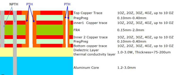
Furthermore, the number of layers in a PCB can influence the optimal thickness.
Multilayer PCBs, which are commonly used in complex electronic systems, require careful consideration of layer stack-up and overall thickness. Each additional layer increases the total thickness of the PCB, and the spacing between layers must be sufficient to accommodate vias and other interconnections. Therefore, when designing multilayer PCBs, it is crucial to collaborate closely with your PCB manufacturer to ensure that the chosen thickness meets both electrical and mechanical requirements.
In conclusion, selecting the right PCB thickness for your project involves a careful evaluation of mechanical strength, electrical performance, thermal management, and the number of layers. By considering these factors and understanding the trade-offs involved, you can make an informed decision that optimizes the performance and reliability of your final product. Consulting with experienced PCB manufacturers and leveraging their expertise can further enhance your ability to choose the most suitable PCB thickness for your specific application.
Impact Of PCB Thickness On Signal Integrity
The impact of PCB thickness on signal integrity is a critical consideration in the design and manufacturing of printed circuit boards (PCBs). Signal integrity refers to the quality and reliability of electrical signals as they travel through the PCB. Various factors influence signal integrity, including the thickness of the PCB, which can significantly affect the performance of high-speed electronic circuits.
To begin with, PCB thickness directly influences the impedance of the signal traces.
Impedance is the resistance that an electrical signal encounters as it travels through a conductor. For high-frequency signals, maintaining a consistent impedance is crucial to prevent signal reflections and losses. Thicker PCBs tend to have higher impedance, which can lead to signal degradation if not properly managed. Conversely, thinner PCBs can offer lower impedance, but they may also be more susceptible to mechanical stress and warping.
Moreover, the dielectric constant of the PCB material, which is affected by its thickness, plays a vital role in signal propagation.
The dielectric constant determines how much the material can store electrical energy. A higher dielectric constant can slow down signal propagation, leading to timing issues in high-speed circuits. Thicker PCBs generally have a higher dielectric constant, which can adversely affect signal speed and timing. Therefore, designers must carefully select the PCB thickness to balance signal speed and integrity.
In addition to impedance and dielectric constant, PCB thickness also impacts the crosstalk between adjacent signal traces.
Crosstalk occurs when a signal in one trace induces an unwanted signal in a neighboring trace, leading to interference and potential data corruption. Thicker PCBs can provide better isolation between traces, reducing the likelihood of crosstalk. However, this benefit must be weighed against the potential drawbacks of increased impedance and dielectric constant.
Thermal management is another aspect where PCB thickness plays a crucial role.
Thicker PCBs can dissipate heat more effectively, which is essential for maintaining signal integrity in high-power applications. Excessive heat can cause signal distortion and component failure, so adequate thermal management is necessary to ensure reliable operation. However, thicker PCBs may also introduce challenges in terms of manufacturing complexity and cost.
Furthermore, the mechanical properties of the PCB are influenced by its thickness.
Thicker PCBs are generally more robust and less prone to bending or warping, which can be advantageous in applications requiring high mechanical stability. On the other hand, thinner PCBs are more flexible and can be used in compact or flexible electronic devices. The choice of PCB thickness must therefore consider the specific mechanical requirements of the application.
In conclusion, the thickness of a PCB has a profound impact on signal integrity, affecting impedance, dielectric constant, crosstalk, thermal management, and mechanical properties. Designers must carefully balance these factors to optimize the performance and reliability of electronic circuits. By understanding the interplay between PCB thickness and signal integrity, engineers can make informed decisions that enhance the overall functionality and durability of their designs.
Comparing Standard And Custom PCB Thickness Options
Printed Circuit Boards (PCBs) are fundamental components in modern electronic devices, serving as the backbone for electrical connections and mechanical support. One critical aspect of PCB design is the thickness of the board, which can significantly impact the performance, durability, and application of the final product. When comparing standard and custom PCB thickness options, it is essential to consider various factors, including manufacturing processes, material properties, and specific application requirements.
Standard PCB thicknesses are typically 1.6mm, which has become the industry norm due to its balance of mechanical strength and versatility.
This thickness is suitable for a wide range of applications, from consumer electronics to industrial machinery. The 1.6mm thickness provides adequate support for components, ensuring that the board can withstand mechanical stresses during assembly and operation. Additionally, standard thickness PCBs are generally more cost-effective, as they align with the default settings of most manufacturing equipment, reducing production time and material waste.
However, there are scenarios where standard PCB thickness may not meet the specific needs of a project.
In such cases, custom PCB thickness options become invaluable. Custom thicknesses can range from as thin as 0.2mm to as thick as 3.2mm or more, depending on the requirements of the application. For instance, in compact electronic devices such as smartphones and wearable technology, thinner PCBs are often preferred to save space and reduce weight. Conversely, thicker PCBs are advantageous in applications that demand higher mechanical strength and durability, such as automotive and aerospace industries.
Transitioning from standard to custom PCB thickness involves several considerations.
One primary factor is the material used in the PCB. The most common material is FR4, a composite of woven fiberglass cloth with an epoxy resin binder that is flame resistant. While FR4 is versatile and widely used, other materials such as polyimide, Rogers, and metal-core substrates may be selected for custom thickness PCBs to meet specific thermal, electrical, or mechanical requirements. Each material has its unique properties that can influence the overall performance of the PCB, making the choice of material a critical decision in the design process.
Another important consideration is the impact of PCB thickness on signal integrity and thermal management.
Thicker PCBs can provide better heat dissipation, which is crucial in high-power applications where overheating can lead to component failure. On the other hand, thinner PCBs may offer improved signal integrity by reducing the distance between layers, thereby minimizing signal loss and electromagnetic interference. Designers must carefully evaluate these factors to ensure that the chosen PCB thickness aligns with the performance criteria of the final product.
Moreover, the manufacturing process for custom thickness PCBs can be more complex and time-consuming compared to standard thickness boards.
Custom thicknesses may require specialized equipment and additional steps in the fabrication process, potentially leading to higher production costs and longer lead times. It is essential for designers to collaborate closely with PCB manufacturers to understand the implications of custom thickness on the overall production timeline and budget.
In conclusion, while standard PCB thicknesses offer a cost-effective and versatile solution for many applications, custom PCB thickness options provide the flexibility to meet specific design and performance requirements. By carefully considering factors such as material properties, signal integrity, thermal management, and manufacturing processes, designers can make informed decisions that optimize the functionality and reliability of their electronic devices.


