PCB Via Technology: A Comprehensive Guide
Introduction to PCB Vias
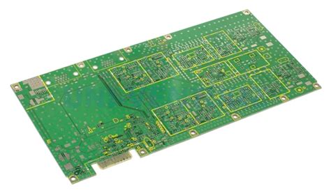
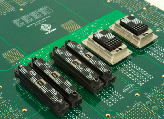
Printed Circuit Board (PCB) via technology represents one of the most critical aspects of modern electronics manufacturing. As electronic devices continue to shrink in size while increasing in complexity, the role of vias in facilitating reliable interconnections between different layers of a PCB has become increasingly important. A via is essentially a conductive hole that allows electrical signals to pass from one layer of a PCB to another, enabling the three-dimensional routing that makes today’s high-density designs possible.
The evolution of via technology has paralleled the advancement of PCB manufacturing techniques. From simple through-hole vias to sophisticated microvias and buried structures, the variety of via types now available allows designers to optimize their boards for performance, reliability, and cost. This article explores the various types of PCB vias, their manufacturing processes, design considerations, and emerging trends in via technology.
Types of PCB Vias
Through-Hole Vias
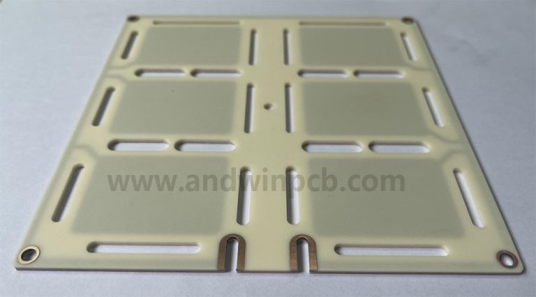
Through-hole vias are the most basic and commonly used type in PCB manufacturing. These vias extend from the top layer to the bottom layer of the board, completely penetrating the substrate. Characterized by their relatively large size (typically 0.2mm to 0.5mm in diameter), through-hole vias offer excellent reliability and ease of manufacturing. They are particularly suitable for double-sided boards and simpler multilayer designs where high density isn’t a primary concern.
The manufacturing process for through-hole vias involves drilling holes through the entire board after layer stacking, followed by plating to create the conductive barrel. While cost-effective and robust, through-hole vias occupy significant board space and can limit routing density in complex designs.

Blind Vias
Blind vias represent a more advanced interconnect solution, connecting an outer layer to one or more inner layers without passing through the entire board. These vias are visible from only one side of the PCB, hence the term “blind.” Typically smaller in diameter than through-hole vias (often 0.1mm to 0.3mm), blind vias enable higher component density by freeing up space on layers they don’t access.
The fabrication of blind vias requires more sophisticated processes such as laser drilling or sequential lamination. While more expensive to produce than through-hole vias, blind vias offer significant advantages in high-density interconnect (HDI) designs where space optimization is crucial.
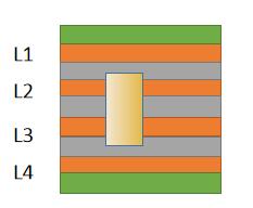
Buried Vias
Buried vias exist entirely within the inner layers of a PCB, with no connection to either outer surface. These completely concealed interconnects allow for complex routing schemes between internal layers without consuming valuable surface real estate. Buried vias are particularly valuable in sophisticated multilayer boards (typically 8 layers or more) where signal routing between intermediate layers is necessary.
The manufacturing process for buried vias involves creating the vias in individual sub-composites before final board lamination. This sequential build-up approach increases production complexity and cost but provides unparalleled routing flexibility for advanced designs.
Microvias
Microvias represent the cutting edge of via technology, defined as vias with a diameter of 0.15mm or less. These tiny interconnects are essential for modern HDI designs, enabling the ultra-fine pitch required for advanced package technologies like ball grid arrays (BGAs) and chip-scale packages (CSPs). Microvias are typically created using laser drilling rather than mechanical methods due to their small size.
There are several microvia configurations:
- Stacked microvias (vertically aligned)
- Staggered microvias (offset vertically)
- Skip vias (spanning multiple layers)
Microvias allow for significantly increased routing density but require careful design to ensure reliability, particularly with regard to thermal stress management.
Via Manufacturing Processes
Mechanical Drilling
Traditional mechanical drilling remains the most common method for creating through-hole vias and larger blind/buried vias. High-speed spindle drills with carbide bits can create holes as small as 0.15mm, though typical production vias are larger for reliability. Mechanical drilling is cost-effective for standard via sizes but faces limitations with smaller diameters and certain materials.
Laser Drilling
Laser drilling has become essential for microvia creation, capable of producing holes as small as 0.025mm. CO2 and UV lasers are commonly used, each with advantages for different materials. Laser drilling offers precision and speed for high-density designs but requires careful parameter control to avoid thermal damage to surrounding materials.
Plating Techniques
After hole creation, vias must be plated to establish conductivity. Electrolytic copper plating is standard, though alternative approaches like conductive inks are emerging. The plating process must ensure uniform coverage throughout the via barrel, particularly challenging for high aspect ratio vias. Recent advances in pulse plating and direct metallization have improved plating quality in demanding applications.
Filling and Capping
Many advanced applications require vias to be filled with conductive or non-conductive material, then capped with copper. Via filling improves thermal performance, provides planar surfaces for fine-pitch components, and enhances reliability by preventing air entrapment. Various filling materials are used including conductive epoxies, copper paste, and resin systems.
Design Considerations for PCB Vias
Aspect Ratio
The aspect ratio (depth to diameter) of a via significantly impacts its manufacturability and reliability. Traditional through-hole vias typically maintain aspect ratios below 10:1, while microvias are designed with much lower ratios (often 0.75:1) for improved reliability. High aspect ratio vias present challenges for plating uniformity and may require specialized processes.
Thermal Management
Vias play a crucial role in PCB thermal management, particularly for power electronics and high-current applications. Thermal vias are specifically designed to conduct heat away from components to other layers or heatsinks. The arrangement, quantity, and plating thickness of thermal vias must be carefully calculated to achieve desired thermal performance.
Signal Integrity
For high-speed designs, via characteristics can significantly impact signal quality. Stub effects in through-hole vias can cause signal reflections, while impedance discontinuities at via transitions may degrade signal integrity. Techniques like back-drilling (removing unused via portions) and careful via placement help maintain signal quality in sensitive circuits.
Reliability Considerations
Via reliability is critical for product longevity, particularly in harsh environments. Thermal cycling can cause fatigue failures in poorly designed vias. Factors like plating quality, via geometry, and material compatibility must be considered to ensure long-term reliability. Accelerated life testing is often employed to validate via designs for demanding applications.
Advanced Via Technologies and Future Trends
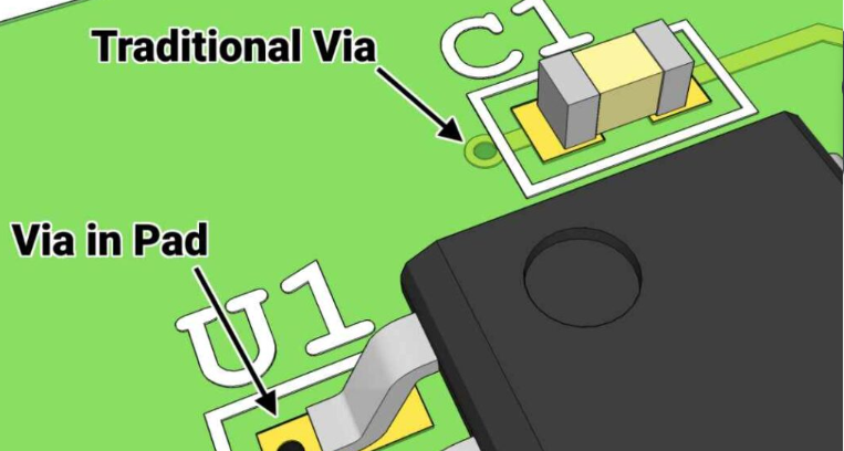
Via-in-Pad Technology
Via-in-pad places vias directly in component pads, saving space and improving high-frequency performance by minimizing lead lengths. This technique requires precise filling and planarization to prevent solder wicking during assembly. Via-in-pad is increasingly common in BGA and fine-pitch component applications.
3D Printed Electronics
Additive manufacturing techniques are enabling new via formation methods. 3D printed electronics can create complex via structures not possible with traditional subtractive processes, including curved and shaped interconnects. While still emerging, this technology promises new possibilities for PCB design.
Embedded Component Technology
The integration of passive and active components within the PCB substrate relies heavily on advanced via technologies. These embedded designs require sophisticated via structures to interconnect buried components while maintaining signal integrity and thermal performance.
Photonic Via Technology
As high-speed designs push into the millimeter-wave and terahertz ranges, photonic vias that can handle both electrical and optical signals are under development. These hybrid structures may play a crucial role in future high-bandwidth communication systems.
Conclusion
PCB via technology continues to evolve to meet the demands of increasingly sophisticated electronic systems. From basic through-hole interconnects to advanced microvia architectures, the humble via remains a critical enabler of modern electronics miniaturization and performance. As emerging technologies like 5G, IoT, and artificial intelligence drive the need for more complex and dense circuit boards, via technology will continue to advance, presenting both new opportunities and challenges for designers and manufacturers alike.
Understanding the various via types, their manufacturing processes, and design considerations is essential for creating reliable, high-performance PCBs. As the industry moves toward even higher densities and more complex multilayer structures, innovations in via technology will play a pivotal role in shaping the future of electronic packaging and interconnection.