PCB vs. PCBA: From Design to Assembly in Modern Electronics
Key Takeaways
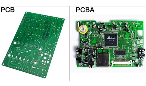
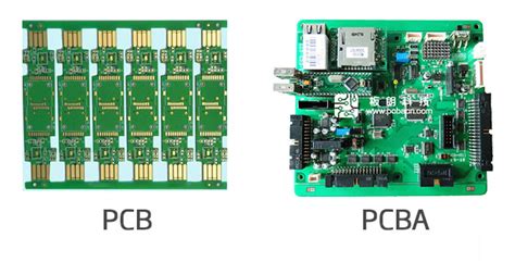
Understanding the fundamental differences between PCB (Printed Circuit Board) and PCBA (Printed Circuit Board Assembly) is critical for navigating modern electronics manufacturing. While a PCB serves as the bare foundation for electronic circuits—comprising conductive pathways etched onto non-conductive substrate—PCBA represents the functional evolution of this base through PCB assembly, where components like resistors, ICs, and connectors are mounted.
The PCB design process begins with schematic creation and layout optimization, focusing on signal integrity and thermal management. In contrast, PCBA introduces complexities like component sourcing, solder paste application, and reflow soldering during PCB assembly. A key distinction lies in their end states: PCB remains inert until populated, while PCBA denotes a fully operational system ready for integration into devices.
For manufacturers, timing and precision define success. PCB assembly requires meticulous coordination between design files, automated pick-and-place machines, and quality testing protocols. Modern PCBA systems further emphasize miniaturization, with surface-mount technology (SMT) enabling denser component layouts. As technologies advance, innovations like 3D-printed circuits and AI-driven inspection tools are reshaping both PCB fabrication and PCBA workflows, underscoring the need for adaptability in this dynamic field.
When evaluating projects, engineers must align PCB design choices with PCBA requirements early—such as pad sizing for solder joints or test point placement—to avoid costly rework. This interconnected relationship highlights why mastering the transition from design to assembly remains pivotal in delivering reliable electronic solutions.
PCB and PCBA Core Differences Explained
At the heart of modern electronics manufacturing lies the critical distinction between PCB (Printed Circuit Board) and PCBA (Printed Circuit Board Assembly). While these terms are often used interchangeably, they represent fundamentally different stages in the production of electronic systems. A PCB serves as the foundational platform—a non-conductive substrate laminated with copper traces that form electrical pathways. In contrast, PCBA refers to the fully functional board created after components such as resistors, capacitors, and integrated circuits are mounted and soldered onto the PCB through PCB assembly processes.
"Understanding the transition from bare PCB to functional PCBA is essential for optimizing manufacturing workflows and avoiding costly design errors," notes a senior electronics engineer at a leading OEM.
The core difference hinges on functionality: a PCB remains inert until components are added, while a PCBA embodies the operational heart of devices. PCB assembly bridges this gap, transforming a static board into a dynamic circuit capable of powering everything from smartphones to industrial machinery. Key milestones in this transformation include solder paste application, component placement via pick-and-place machines, and reflow soldering—each requiring precision to ensure electrical continuity and thermal stability.
Another critical distinction lies in testing protocols. Bare PCBs undergo electrical testing to verify trace integrity, whereas PCBA validation focuses on functional performance, including power-on tests and signal integrity analysis. This phased approach ensures defects are caught early, reducing rework costs.
Tip: Designers should collaborate closely with PCB assembly teams to align component footprints with manufacturing capabilities, minimizing placement errors during PCBA stages.
By recognizing these differences, engineers can better navigate the transition from schematic design to a fully realized PCBA, ensuring both technical rigor and cost efficiency in electronics production.
PCBA Assembly Stages in Electronics Production
The transformation from a bare PCB to a functional PCBA involves a meticulously orchestrated sequence of manufacturing stages. Unlike PCB assembly, which focuses solely on board fabrication, PCBA encompasses the integration of electronic components to create operational circuitry. This critical phase begins with solder paste application, where a stencil deposits precise amounts of solder onto designated pads. Automated pick-and-place systems then position surface-mount devices (SMDs) with micron-level accuracy, ensuring alignment with the board’s design specifications.
Following component placement, the assembly enters reflow soldering, a thermal process that melts the solder paste to form permanent electrical connections. Modern reflow ovens utilize carefully calibrated temperature profiles to prevent thermal stress on sensitive components. For boards requiring mixed-technology assembly, through-hole components are manually or mechanically inserted post-reflow, followed by wave soldering to secure their leads.
Automated optical inspection (AOI) systems scan the PCBA for defects such as misaligned parts, solder bridges, or insufficient joints. Advanced manufacturers supplement AOI with X-ray inspection to verify hidden connections in ball-grid-array (BGA) packages. The final steps involve functional testing, where the assembled board undergoes simulated operational conditions to validate performance metrics like signal integrity and power distribution.
Throughout these stages, traceability protocols ensure component authenticity and process compliance, particularly for industries like aerospace or medical electronics. By harmonizing precision machinery with rigorous quality checks, PCBA production bridges the gap between circuit design and real-world functionality, delivering robust assemblies ready for integration into end-use devices.
Circuit Board Development: Prototype to Assembly
The journey from PCB prototype to full PCBA integration represents a critical evolution in electronics manufacturing. Prototyping begins with design verification, where engineers test circuit layouts using specialized software like Altium Designer or KiCad. This stage focuses on identifying potential flaws in signal integrity, thermal management, and component placement before committing to physical production. Modern rapid prototyping techniques, such as laser-direct imaging (LDI), enable the creation of functional PCB assembly test units within 24–48 hours, significantly accelerating development cycles.
Transitioning to PCBA introduces a layered manufacturing approach. Prototype assemblies typically use manual or semi-automated soldering for flexibility, allowing engineers to evaluate component interactions and power distribution under real-world conditions. Once validated, the design progresses to volume production, where surface-mount technology (SMT) lines place thousands of microcomponents per hour with sub-millimeter precision. A key differentiator between prototype and mass-produced PCBA lies in the implementation of Design for Manufacturability (DFM) principles, which optimize layouts for automated assembly while minimizing solder bridging or tombstoning risks.
Quality assurance bridges these phases, with advanced inspection systems like automated optical inspection (AOI) and X-ray imaging verifying solder joint integrity across both PCB assembly stages. For high-frequency or high-power applications, engineers often incorporate signal integrity testing and thermal stress analysis during prototype PCBA evaluation. This dual-phase development model ensures that final products meet rigorous performance standards while maintaining scalability—critical for industries ranging from consumer electronics to aerospace systems.
The shift from prototype to full-scale PCBA production also demands material considerations. While prototypes may use standard FR-4 substrates, volume manufacturing frequently employs specialized laminates with improved thermal conductivity or reduced dielectric loss. This progression underscores the importance of collaborative workflows between design engineers and PCB assembly technicians, ensuring seamless transitions from concept to functional electronic systems.
Component Integration in Modern PCBA Systems
The evolution of PCBA (Printed Circuit Board Assembly) systems has redefined how electronic components are strategically placed and interconnected on bare PCB substrates. Unlike traditional methods that treated component mounting as a separate phase, modern integration approaches emphasize design-for-manufacturing principles from the outset. Engineers now leverage advanced PCB assembly techniques such as surface-mount technology (SMT) and mixed-technology layouts to accommodate components ranging from nanometer-scale ICs to high-power modules within the same board architecture.
A critical shift lies in the synchronization between automated pick-and-place systems and 3D solder paste inspection, enabling precise alignment of miniature components like 01005 resistors or wafer-level chip-scale packages. This precision is further enhanced by thermal profiling during reflow soldering, which ensures reliable electrical connections without compromising component integrity. For hybrid designs combining SMT and through-hole components, PCBA workflows now incorporate selective wave soldering to maintain process efficiency while handling diverse form factors.
The rise of high-density interconnect (HDI) boards has intensified the focus on stackup optimization and material selection. Modern systems prioritize low-loss dielectrics and controlled-impedance traces to support high-frequency signals in 5G modules or AI accelerators. Additionally, embedded component technology allows passive elements like resistors and capacitors to be laminated within the PCB itself, reducing surface area usage by up to 40% compared to conventional assemblies.
However, this integration complexity demands rigorous design rule checks (DRC) and manufacturing execution systems (MES) to prevent defects in densely packed layouts. Advanced PCBA providers now employ automated optical inspection (AOI) paired with X-ray tomography to verify solder joint quality under Ball Grid Array (BGA) components or hidden interconnects. As IoT and wearable technologies push miniaturization limits, the industry is adopting panel-level packaging and flex-rigid PCB assemblies to balance component density with mechanical reliability—a paradigm reshaping how engineers approach space-constrained applications in medical devices and automotive electronics.
Electronics Manufacturing Workflow Analysis
The journey from conceptual design to functional electronic devices hinges on a meticulously orchestrated PCB assembly process. Modern electronics manufacturing workflows typically unfold in two distinct phases: fabrication of the bare printed circuit board (PCB) and its subsequent transformation into a populated PCBA (Printed Circuit Board Assembly). This dual-stage approach ensures precision while accommodating the complex interplay between hardware design and component integration.
Workflow initiation begins with PCB fabrication, where design files guide the creation of copper-clad substrates through photolithography and etching processes. Advanced manufacturers employ automated optical inspection (AOI) systems at this stage to verify trace integrity and hole alignment. Upon successful fabrication, the workflow transitions into PCBA operations, where surface-mount technology (SMT) and through-hole components are strategically placed.
Critical workflow milestones include:
- Solder paste stenciling for precise component adhesion
- High-speed pick-and-place machinery positioning up to 30,000 components per hour
- Reflow soldering profiles optimized for diverse component thermal requirements
- Post-assembly functional testing simulating real-world operating conditions
Contemporary PCB assembly lines integrate Industry 4.0 principles, with machine learning algorithms predicting solder joint quality and IoT-enabled trackers monitoring production bottlenecks. This technological synergy reduces time-to-market while maintaining PCBA reliability standards.
Workflow optimization challenges persist, particularly in balancing thermal management needs with component density in advanced PCBA configurations. Manufacturers increasingly adopt just-in-time material delivery systems and cross-functional digital twins to synchronize design intent with assembly realities, creating a cohesive manufacturing continuum from bare PCB to operational PCBA.
Quality Control for PCB vs PCBA Projects
Effective quality assurance protocols differ significantly between PCB fabrication and PCBA processes, reflecting their distinct manufacturing stages. For bare board inspection, PCB quality control focuses on material integrity, trace width accuracy, and surface finish consistency. Automated optical inspection (AOI) systems scan for defects like micro-cracks or copper layer irregularities, ensuring compliance with IPC-A-600 standards.
In contrast, PCBA quality control introduces multi-layered verification for component placement accuracy, solder joint reliability, and electrical functionality. Post-PCB assembly, inline testing combines AOI with X-ray inspection to detect hidden flaws such as voids in BGA solder balls or misaligned QFN packages. Functional testing becomes critical at this stage, simulating real-world operating conditions to validate circuit performance.
While environmental stress testing (e.g., thermal cycling) applies to both PCB and PCBA phases, the latter requires stricter electromagnetic compatibility checks to prevent signal interference in populated boards. Manufacturers often employ statistical process control (SPC) to monitor PCB assembly yield rates, addressing deviations in solder paste deposition or reflow oven profiles.
The interdependence of these quality systems underscores a fundamental truth: a flawless PCB design becomes irrelevant if PCBA processes compromise component integration. By aligning inspection protocols with stage-specific risks, electronics producers mitigate failures that could escalate costs at later production stages.
Emerging Technologies in Board Assembly
The evolution of PCB assembly techniques has entered a transformative phase, driven by innovations that address the growing complexity of modern electronics. One breakthrough lies in automated optical inspection (AOI) systems, which leverage machine vision to detect micro-scale defects in PCBA during high-speed production. These systems now incorporate AI algorithms capable of learning from historical defect patterns, reducing false positives by over 40% compared to traditional methods.
Another advancement reshaping PCB assembly is the integration of 3D printing technologies for rapid prototyping. Manufacturers now employ additive manufacturing to create multilayer board substrates with embedded components, compressing development cycles from weeks to days. This approach proves particularly valuable for high-density interconnect (HDI) designs, where precision placement of micro-components is critical.
The rise of industrial IoT has also revolutionized PCBA workflows. Smart factories utilize sensor-equipped assembly lines that monitor solder paste viscosity, reflow oven temperature profiles, and component placement accuracy in real time. This data-driven approach enables predictive maintenance, with some facilities reporting a 30% reduction in equipment downtime.
Advanced laser direct structuring (LDS) techniques are pushing the boundaries of component integration. By selectively activating circuit paths on thermoplastic substrates, this method allows for three-dimensional PCB assembly configurations that traditional planar boards cannot achieve. Paired with conductive inkjet printing, it enables the creation of flexible hybrid circuits for wearable tech and IoT devices.
Emerging quantum dot soldering methods address the challenges of miniaturization in PCBA, offering sub-100-micron joint formations with enhanced thermal stability. These nanocrystalline alloys maintain conductivity at higher temperatures while reducing electromigration risks in high-frequency applications.
As sustainability pressures mount, novel bio-based flux formulations and lead-free solder alloys are gaining traction in PCB assembly processes. These materials not only comply with tightening environmental regulations but also demonstrate comparable performance to conventional counterparts in stress-test scenarios.
The convergence of these technologies creates a paradigm shift where PCBA evolves from discrete manufacturing stages to a seamless, intelligent production ecosystem. This technological leap ensures electronics manufacturers can meet the dual demands of increased functionality and accelerated time-to-market in an era of smart, connected devices.
Conclusion
The journey from PCB design to PCBA represents a critical pathway in modern electronics manufacturing, underscoring the symbiotic relationship between conceptual design and functional realization. While PCB assembly focuses on the meticulous placement of components onto a bare board, PCBA encompasses the complete process of transforming a static substrate into an operational electronic system. This distinction highlights the importance of precision at every stage—from schematic validation to solder paste application and component soldering.
As technology evolves, advancements in automated optical inspection (AOI) and surface-mount technology (SMT) continue to refine both PCB fabrication and PCBA workflows. Manufacturers now prioritize design-for-manufacturability (DFM) principles to bridge the gap between prototyping and mass production, ensuring compatibility across design software and assembly machinery. The integration of IoT-enabled testing protocols further strengthens quality assurance, addressing potential defects in PCB assembly before final product integration.
Ultimately, the transition from PCB to PCBA reflects the electronics industry’s commitment to innovation and reliability. By harmonizing design intent with assembly execution, engineers can optimize performance while mitigating risks associated with component misalignment or thermal stress. As emerging technologies like flexible hybrid electronics (FHE) gain traction, the collaboration between PCB designers and PCBA specialists will remain pivotal in shaping next-generation electronic devices—balancing complexity, scalability, and cost-efficiency from prototyping to full-scale deployment.
Frequently Asked Questions
What distinguishes a PCB from a PCBA in electronics manufacturing?
A PCB (Printed Circuit Board) refers to the bare board with conductive pathways etched onto it, while a PCBA (Printed Circuit Board Assembly) represents the fully assembled board with components like resistors, capacitors, and ICs soldered onto it. The transition from PCB to PCBA occurs during the pcb assembly stage, where components are integrated to create a functional circuit system.
How does the design process differ between PCB and PCBA development?
PCB design focuses on layout optimization, layer stacking, and ensuring electrical connectivity through traces. In contrast, PCBA design involves component placement, thermal management, and compatibility with automated assembly equipment. The pcb assembly phase bridges these two stages, transforming the static board into an operational electronic device.
What critical steps are involved in modern PCBA assembly?
The pcb assembly process typically includes solder paste application, component placement via pick-and-place machines, reflow soldering, and rigorous testing. Advanced PCBA systems now incorporate automated optical inspection (AOI) and X-ray verification to ensure precision, especially for high-density interconnects or miniaturized components.
Why is quality control more complex for PCBA compared to bare PCBs?
While PCB quality checks focus on electrical continuity and mechanical integrity, PCBA testing evaluates functional performance, component alignment, and solder joint reliability. Defects in pcb assembly, such as tombstoning or cold joints, require specialized diagnostics, making PCBA quality assurance a multi-layered process.
How do emerging technologies impact PCB and PCBA manufacturing?
Innovations like flexible hybrid electronics (FHE) and embedded components are reshaping both PCB design and pcb assembly methodologies. For PCBA, advancements in 3D printing and AI-driven inspection systems are accelerating prototyping cycles while reducing error rates in high-volume production.
Explore Custom PCB Assembly Solutions
For tailored pcb assembly services that align with your project’s technical requirements, please click here to consult with our engineering team. From prototyping to full-scale PCBA production, we ensure precision at every stage of your electronics manufacturing workflow.


