Pcb vs Pwb
Differences Between PCB VS PWB: A Comprehensive Guide
Printed Circuit Boards (PCBs) and Printed Wiring Boards (PWBs) are terms often used interchangeably in the electronics industry, yet they denote distinct concepts that are crucial to understand for anyone involved in electronic design and manufacturing. To begin with, it is essential to recognize that both PCBs and PWBs serve as foundational components in electronic devices, providing the necessary platform for mounting and interconnecting various electronic components. However, the differences between them lie in their scope, functionality, and the context in which they are used.
Firstly, the term Printed Circuit Board (PCB) is more encompassing and widely recognized in the industry.
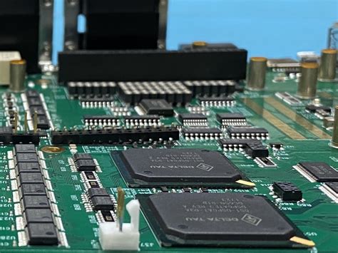
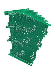
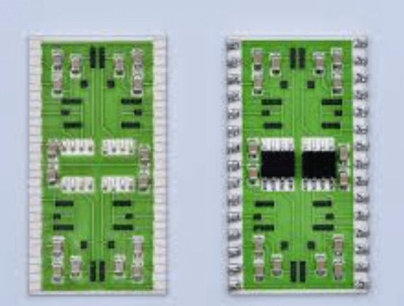
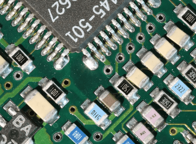
A PCB refers to a board that not only contains the wiring or traces to connect electronic components but also includes the components themselves, such as resistors, capacitors, and integrated circuits. PCBs are integral to the functionality of electronic devices, as they facilitate the flow of electrical signals and power between components, ensuring the device operates as intended.
The design and manufacturing of PCBs involve multiple layers, including a substrate, conductive pathways, and often a protective solder mask. This complexity allows for the creation of sophisticated electronic circuits that can perform a wide range of functions.
In contrast, a Printed Wiring Board (PWB) is a more specific term that refers solely to the board with the printed wiring or traces, without the inclusion of electronic components. Essentially, a PWB is a precursor to a PCB. It provides the physical structure and the electrical pathways needed for the assembly of a complete circuit but does not encompass the components themselves. PWBs are typically used in the initial stages of electronic design and prototyping, where the focus is on establishing the correct layout and connections before the components are added. This distinction is crucial for understanding the different stages of electronic manufacturing and the terminology used in each phase.
Moreover, the terminology can also reflect historical and regional differences.
The term PWB was more commonly used in the early days of electronic manufacturing when the focus was primarily on the wiring aspect of the boards. As technology advanced and the integration of components onto the boards became more prevalent, the term PCB gained prominence. Today, PCB is the more universally accepted term, especially in the context of modern electronics where the integration of components is a given.
Another key difference lies in the applications and industries where these terms are used.
PCBs are ubiquitous in consumer electronics, telecommunications, automotive, and aerospace industries, among others. They are essential for the operation of devices ranging from smartphones and computers to complex avionics systems. On the other hand, PWBs might be more commonly referenced in specialized fields such as research and development, where the focus is on the design and testing of new circuit layouts before full-scale production.
In conclusion, while PCBs and PWBs are closely related and often used interchangeably, understanding their differences is vital for anyone involved in electronic design and manufacturing.
PCBs represent the complete assembly of a circuit, including both the wiring and the components, whereas PWBs refer specifically to the board with the printed wiring. Recognizing these distinctions not only clarifies the terminology but also provides insight into the various stages and considerations involved in creating electronic devices. As technology continues to evolve, the precise use of these terms will remain important for clear communication and effective collaboration within the industry.
PCB vs PWB: Which One Should You Choose for Your Project?
When embarking on an electronics project, one of the critical decisions you will face is choosing between a Printed Circuit Board (PCB) and a Printed Wiring Board (PWB). Although these terms are often used interchangeably, they have distinct differences that can significantly impact the performance, cost, and complexity of your project. Understanding these differences is essential for making an informed decision.
To begin with, a Printed Circuit Board (PCB) is a board used to mechanically support and electrically connect electronic components using conductive pathways, or traces, etched from copper sheets laminated onto a non-conductive substrate.
PCBs are ubiquitous in modern electronics, from simple gadgets to complex computing systems. They offer several advantages, including high reliability, ease of mass production, and the ability to support complex circuits. The use of PCBs can also lead to reduced electronic noise and improved signal integrity, which are crucial for high-frequency applications.
On the other hand, a Printed Wiring Board (PWB) is essentially an earlier term used to describe what we now commonly refer to as a PCB.
Historically, PWBs were simpler and primarily focused on the wiring aspect, where the emphasis was on creating a physical layout for connecting various components. Over time, as technology advanced, the term PCB became more prevalent, reflecting the broader functionality and complexity of modern boards. Despite this evolution, some industries and professionals still use the term PWB, particularly in contexts where the focus remains on the wiring rather than the circuit complexity.
When deciding between a PCB and a PWB for your project, it is crucial to consider the specific requirements and constraints of your application.
For instance, if your project involves high-frequency signals or requires a high level of integration, a PCB is likely the better choice due to its superior performance characteristics. PCBs can accommodate multiple layers, allowing for more intricate designs and better management of electromagnetic interference (EMI). This makes them ideal for applications such as telecommunications, computing, and advanced consumer electronics.
Conversely, if your project is relatively simple and cost is a significant concern, a PWB might suffice.
PWBs are generally less expensive to produce, especially for low-volume or prototype runs. They can be an excellent choice for straightforward applications where the primary goal is to establish basic electrical connections without the need for advanced features or high-density layouts. Examples include basic household appliances, simple control systems, and educational kits.
Another factor to consider is the manufacturing process.
PCBs typically require more sophisticated fabrication techniques, including photolithography, plating, and etching, which can increase both the cost and lead time. PWBs, being simpler, often involve less complex manufacturing processes, which can be advantageous for quick turnaround times and lower production costs.
In conclusion, the choice between a PCB and a PWB hinges on the specific needs of your project. While PCBs offer advanced capabilities and are suitable for complex, high-performance applications, PWBs provide a cost-effective solution for simpler projects. By carefully evaluating the requirements, constraints, and goals of your project, you can make an informed decision that balances performance, cost, and complexity, ensuring the success of your electronic endeavor.
The Evolution of PCB and PWB in Modern Electronics
In the realm of modern electronics, the terms PCB (Printed Circuit Board) and PWB (Printed Wiring Board) are often used interchangeably, yet they denote distinct concepts that have evolved significantly over time. Understanding the evolution of these components is crucial for appreciating their roles in contemporary electronic devices.
Initially, the term PWB was more prevalent, referring specifically to the physical board that housed the wiring for electronic circuits.
PWBs were primarily concerned with the layout and connection of wires, serving as a foundational platform for electronic components. The focus was on creating a reliable and efficient means of connecting various electronic parts without the need for complex and cumbersome wiring systems. This innovation marked a significant leap from earlier methods, which relied heavily on manual wiring and point-to-point connections, often resulting in bulky and less reliable assemblies.
As technology advanced, the concept of the PWB began to evolve.
The introduction of the PCB marked a pivotal moment in the history of electronic design and manufacturing. Unlike PWBs, PCBs incorporated not only the wiring but also the mounting of electronic components directly onto the board. This integration allowed for more compact, efficient, and reliable electronic assemblies. The term PCB thus came to represent a more comprehensive approach to circuit board design, encompassing both the wiring and the components themselves.
One of the key innovations that facilitated the transition from PWB to PCB was the development of photolithography techniques.
These techniques enabled the precise etching of intricate circuit patterns onto the board, allowing for greater complexity and miniaturization of electronic circuits. This advancement was instrumental in the proliferation of modern electronic devices, from consumer electronics to industrial applications.
Moreover, the materials used in PCB manufacturing have also evolved.
Early PWBs were typically made from materials like bakelite or phenolic resin, which, while functional, had limitations in terms of durability and performance. The advent of fiberglass-reinforced epoxy laminates, such as FR-4, revolutionized PCB manufacturing by providing a more robust and reliable substrate. These materials offered superior mechanical strength, thermal stability, and electrical insulation properties, making them ideal for high-performance electronic applications.
In addition to material advancements, the methods of component attachment have also progressed.
Surface mount technology (SMT) has largely supplanted through-hole technology, allowing for even greater miniaturization and complexity in PCB design. SMT components are mounted directly onto the surface of the board, eliminating the need for drilling holes and enabling more efficient use of space. This shift has been critical in the development of modern electronics, where compactness and performance are paramount.
Furthermore, the evolution from PWB to PCB has been accompanied by significant advancements in design software and manufacturing processes.
Computer-aided design (CAD) tools have become indispensable in PCB design, allowing engineers to create highly intricate and optimized circuit layouts with precision and efficiency. Automated manufacturing processes, such as pick-and-place machines and reflow soldering, have further streamlined PCB production, ensuring high quality and consistency in mass production.
In conclusion, the evolution from PWB to PCB represents a remarkable journey in the field of electronics. While PWBs laid the groundwork for modern circuit board technology, the advent of PCBs has transformed the landscape, enabling the creation of increasingly sophisticated and compact electronic devices. This evolution continues to drive innovation, shaping the future of electronics and paving the way for new advancements in technology.
Cost Comparison: PCB vs PWB in Manufacturing
When evaluating the cost implications of manufacturing Printed Circuit Boards (PCBs) versus Printed Wiring Boards (PWBs), it is essential to consider several factors that influence the overall expenditure. Both PCBs and PWBs serve as foundational components in electronic devices, yet they differ in complexity, materials, and manufacturing processes, which in turn affect their cost structures.
To begin with, the primary distinction between PCBs and PWBs lies in their design and functionality.
PCBs are more advanced, incorporating multiple layers and complex circuitry, which allows for greater functionality and integration of components. In contrast, PWBs are typically simpler, often consisting of a single layer of conductive material. This fundamental difference in design complexity directly impacts the cost of production. PCBs, due to their intricate design, require more sophisticated manufacturing techniques and equipment, leading to higher initial setup costs. Conversely, the simpler design of PWBs generally results in lower production costs.
Another critical factor influencing the cost is the choice of materials.
PCBs often utilize high-quality substrates such as FR4, which provide excellent thermal and electrical properties but come at a higher price point. Additionally, the use of advanced materials like high-frequency laminates or flexible substrates in PCBs can further escalate costs. On the other hand, PWBs typically use less expensive materials, which contribute to their lower overall cost. The selection of materials not only affects the direct cost but also impacts the durability and performance of the final product, which must be considered when making a cost comparison.
Furthermore, the manufacturing process itself plays a significant role in determining the cost.
The production of PCBs involves multiple stages, including drilling, plating, and etching, each requiring specialized equipment and skilled labor. These processes are time-consuming and add to the overall cost. In contrast, the manufacturing of PWBs is relatively straightforward, often involving fewer steps and less sophisticated machinery. This simplicity translates to reduced labor costs and shorter production times, making PWBs a more cost-effective option for certain applications.
In addition to the direct costs associated with materials and manufacturing, it is important to consider the economies of scale.
For large production runs, the cost per unit of PCBs can decrease significantly due to the distribution of setup costs over a larger number of units. However, for smaller production runs, the high initial setup costs of PCBs can make them less economical compared to PWBs. This scalability factor is crucial for manufacturers to consider when deciding between PCBs and PWBs for their specific needs.
Moreover, the end-use application of the boards also influences the cost decision.
PCBs, with their advanced capabilities, are often required in high-performance and high-reliability applications such as aerospace, medical devices, and telecommunications. In these cases, the higher cost of PCBs is justified by the need for superior performance and reliability. On the other hand, PWBs are suitable for simpler, cost-sensitive applications where the advanced features of PCBs are not necessary. This differentiation in application further underscores the importance of aligning the choice of board with the specific requirements of the project.
In conclusion, while PCBs generally incur higher costs due to their complexity, advanced materials, and sophisticated manufacturing processes, PWBs offer a more economical alternative for simpler applications. The decision between PCBs and PWBs should be guided by a thorough analysis of design requirements, material selection, production volume, and end-use application. By carefully considering these factors, manufacturers can make informed decisions that balance cost with performance and reliability.