Pcb wipe sample procedure
Understanding The Basics Of PCB Wipe Sample Procedures
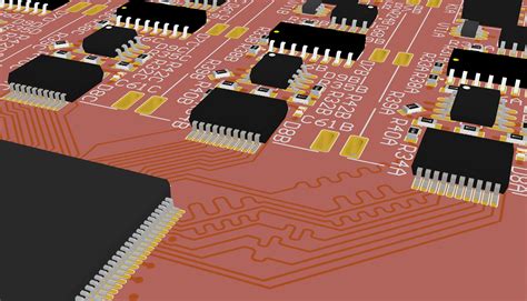
Printed Circuit Boards (PCBs) are integral components in modern electronic devices, serving as the backbone for electrical connections and functionality. Ensuring their cleanliness and integrity is paramount, particularly in industries where precision and reliability are critical.
One method employed to assess the cleanliness of PCBs is the wipe sample procedure.
This process is essential for detecting contaminants that may compromise the performance and longevity of electronic devices. Understanding the basics of PCB wipe sample procedures involves recognizing the importance of cleanliness, the methodology employed, and the interpretation of results.
To begin with, the significance of maintaining clean PCBs cannot be overstated.
Contaminants such as dust, oils, and residues from manufacturing processes can lead to electrical failures, corrosion, and reduced performance. Therefore, regular monitoring and cleaning are necessary to uphold the quality and reliability of PCBs. The wipe sample procedure is a straightforward yet effective method to evaluate the presence of surface contaminants. By employing this technique, manufacturers can ensure that their products meet industry standards and customer expectations.
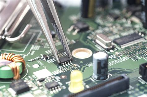
The procedure itself involves several key steps, starting with the selection of appropriate materials.
Typically, a cleanroom-grade wipe, often made of non-abrasive, lint-free material, is used to collect samples from the PCB surface. The choice of solvent is also crucial, as it must effectively dissolve potential contaminants without damaging the PCB. Common solvents include isopropyl alcohol or deionized water, depending on the nature of the contaminants being targeted. Once the materials are prepared, the wipe is moistened with the solvent and gently applied to the PCB surface in a consistent manner, ensuring that all areas are covered.
Following the collection of samples, the next phase involves analyzing the contaminants present on the wipe.
This analysis can be conducted using various techniques, such as gravimetric analysis, ion chromatography, or spectroscopy, each offering different insights into the types and quantities of contaminants. Gravimetric analysis, for instance, measures the total mass of residues collected, providing a general indication of cleanliness. In contrast, ion chromatography can identify specific ionic contaminants, offering a more detailed understanding of potential issues.
Interpreting the results of a PCB wipe sample procedure requires a comprehensive understanding of industry standards and the specific requirements of the application.
Standards such as those set by the IPC (Association Connecting Electronics Industries) provide guidelines on acceptable levels of contaminants for different types of PCBs. By comparing the results against these benchmarks, manufacturers can determine whether their cleaning processes are effective or if further action is needed.
In conclusion, the PCB wipe sample procedure is a vital tool in the maintenance and quality assurance of electronic components. By systematically collecting and analyzing surface contaminants, manufacturers can ensure that their products remain reliable and efficient. This procedure not only helps in identifying potential issues before they escalate but also reinforces the commitment to quality and precision in the electronics industry. As technology continues to advance, the importance of such procedures will only grow, underscoring the need for ongoing diligence and adherence to best practices in PCB manufacturing and maintenance.
Step-By-Step Guide To Conducting A PCB Wipe Sample
Conducting a PCB wipe sample is a critical procedure in environmental testing, particularly when assessing contamination levels of polychlorinated biphenyls (PCBs) on surfaces. This process is essential for ensuring compliance with environmental regulations and safeguarding public health. To begin, it is important to understand the necessary materials and equipment required for an accurate and effective PCB wipe sample. Typically, this includes pre-moistened gauze pads or wipes, a solvent such as hexane or isopropanol, clean gloves, a sample container, and appropriate labeling materials.
Before initiating the sampling process, it is crucial to don clean gloves to prevent contamination of the sample.
The selection of the sampling area is the next step, which should be representative of the surface being tested. It is advisable to delineate a specific area, often a 10 cm by 10 cm square, using a template or measuring tape to ensure consistency and accuracy. Once the area is defined, the pre-moistened gauze pad or wipe should be used to collect the sample.
The technique for wiping is of utmost importance.
The wipe should be unfolded and held flat, applying firm and even pressure. Begin at one corner of the delineated area and wipe in a single direction, ensuring complete coverage of the surface. After reaching the opposite corner, fold the wipe to expose a clean side and repeat the process in a perpendicular direction. This cross-hatch pattern helps to maximize the collection of any PCBs present on the surface.
Upon completion of the wiping process, the gauze pad or wipe should be carefully folded with the sampled side inward to prevent loss of the collected material.
It is then placed into a sample container, which should be immediately sealed to avoid contamination. Proper labeling of the sample container is essential, including details such as the date, time, location, and any other relevant information that may assist in the analysis and interpretation of results.
Transporting the sample to the laboratory should be done promptly, adhering to any specific guidelines for temperature control or handling to preserve the integrity of the sample. In the laboratory, the sample will undergo analysis to determine the concentration of PCBs present. This data is crucial for assessing the level of contamination and making informed decisions regarding remediation or further testing.
Throughout the entire process, maintaining a detailed chain of custody is vital.
This documentation ensures that the sample has been handled correctly and provides a traceable record from collection to analysis. It is also important to adhere to any regulatory guidelines or standards that may apply to PCB sampling in your region, as these can vary and may impact the methodology or reporting requirements.
In conclusion, conducting a PCB wipe sample involves a series of meticulous steps that require attention to detail and adherence to established protocols. By following these procedures, one can ensure the collection of reliable data that is essential for environmental assessments and decision-making. The importance of this process cannot be overstated, as it plays a significant role in protecting both the environment and public health from the harmful effects of PCB contamination.

Common Mistakes To Avoid In PCB Wipe Sampling
In the realm of environmental testing and contamination control, PCB wipe sampling is a critical procedure used to detect and quantify polychlorinated biphenyls (PCBs) on surfaces. However, despite its importance, there are common mistakes that can compromise the accuracy and reliability of the results. Understanding these pitfalls is essential for professionals involved in environmental assessments and remediation efforts.
One frequent error in PCB wipe sampling is the improper selection of sampling materials.
The choice of wipe material can significantly influence the efficiency of PCB collection. It is crucial to use wipes that are specifically designed for PCB sampling, as they are engineered to maximize the collection of contaminants. Using inappropriate materials, such as common household wipes or paper towels, can lead to insufficient sample collection and inaccurate results. Therefore, ensuring that the correct materials are used is a fundamental step in the sampling process.
Another common mistake is the failure to adhere to standardized sampling protocols.
Consistency in the sampling technique is vital to obtain reliable data. Deviations from established procedures, such as varying the pressure applied during wiping or altering the size of the sampled area, can introduce variability and affect the comparability of results. It is essential for technicians to be thoroughly trained and to follow the prescribed protocols meticulously to minimize these inconsistencies.
Moreover, contamination of samples is a prevalent issue that can skew results.
Cross-contamination can occur if sampling equipment is not properly cleaned between uses or if samples are not handled with care. To mitigate this risk, it is imperative to use clean gloves and tools for each sample and to store samples in clean, labeled containers. Additionally, maintaining a clean work environment and avoiding contact with potential sources of contamination are crucial practices to uphold the integrity of the samples.
Furthermore, improper labeling and documentation can lead to confusion and errors in data interpretation.
Each sample must be clearly labeled with relevant information, such as the location, date, and time of collection. Accurate documentation ensures that samples can be traced back to their source and that the data can be correctly analyzed and reported. Neglecting this aspect can result in the misidentification of samples and compromise the entire sampling effort.
In addition to these procedural errors, overlooking the importance of environmental conditions during sampling can also impact results.
Factors such as temperature, humidity, and surface conditions can influence the adherence and collection of PCBs. It is important to consider these variables and, if necessary, adjust the sampling strategy to account for them. For instance, sampling on wet or oily surfaces may require additional steps to ensure effective PCB collection.
Finally, inadequate calibration and maintenance of analytical instruments used for PCB detection can lead to inaccurate measurements. Regular calibration and maintenance are essential to ensure that instruments provide precise and reliable data. Neglecting this aspect can result in erroneous readings and misinterpretation of contamination levels.
In conclusion, while PCB wipe sampling is a valuable tool in environmental assessments, it is fraught with potential pitfalls that can compromise data quality. By being aware of common mistakes such as improper material selection, protocol deviations, contamination, poor documentation, environmental oversight, and instrument neglect, professionals can enhance the accuracy and reliability of their sampling efforts. Through meticulous attention to detail and adherence to best practices, the integrity of PCB wipe sampling can be maintained, ultimately contributing to more effective contamination control and environmental protection.
Importance Of PCB Wipe Sample Procedures In Environmental Safety
In the realm of environmental safety, the significance of PCB (polychlorinated biphenyls) wipe sample procedures cannot be overstated. These procedures are essential for assessing and managing the risks associated with PCB contamination, which poses serious health and environmental hazards. PCBs, once widely used in industrial applications due to their chemical stability and insulating properties, have been identified as persistent organic pollutants. Consequently, they have been banned or restricted in many countries. However, their legacy persists in the environment, necessitating rigorous monitoring and remediation efforts.
To begin with, PCB wipe sample procedures are crucial for identifying the presence and concentration of PCBs on surfaces.
This is particularly important in areas where PCBs were historically used or stored, such as electrical substations, manufacturing facilities, and waste disposal sites. By collecting samples from these surfaces, environmental professionals can determine the extent of contamination and assess the potential risk to human health and the environment. This information is vital for developing effective remediation strategies and ensuring compliance with environmental regulations.
Moreover, the accuracy and reliability of PCB wipe sample procedures are paramount.
These procedures typically involve using a solvent-soaked wipe to collect samples from surfaces suspected of contamination. The samples are then analyzed in a laboratory to quantify the concentration of PCBs. It is essential that these procedures are conducted meticulously to avoid cross-contamination and ensure that the results are representative of the actual conditions. Standardized protocols and guidelines, such as those provided by the Environmental Protection Agency (EPA), help ensure consistency and reliability in sampling methods.
In addition to identifying contamination, PCB wipe sample procedures play a critical role in monitoring the effectiveness of remediation efforts.
After cleanup activities, follow-up sampling is necessary to confirm that PCB levels have been reduced to acceptable levels. This ongoing monitoring is crucial for protecting public health and preventing future exposure. Furthermore, it provides valuable data that can inform future environmental policies and practices, contributing to a broader understanding of PCB behavior in the environment.
Transitioning to the broader implications, the importance of PCB wipe sample procedures extends beyond immediate health and safety concerns.
They are integral to the sustainable management of contaminated sites, which is a key component of environmental stewardship. By accurately assessing and addressing PCB contamination, we can prevent further degradation of ecosystems and protect biodiversity. This aligns with global efforts to promote sustainable development and ensure a healthy environment for future generations.
Additionally, the data obtained from PCB wipe sample procedures can support research and innovation in environmental science.
By analyzing trends and patterns in PCB contamination, scientists can develop new technologies and methods for detection, remediation, and prevention. This continuous improvement in environmental management practices is essential for adapting to emerging challenges and advancing our understanding of complex environmental systems.
In conclusion, PCB wipe sample procedures are a vital tool in the arsenal of environmental safety measures. They provide essential data for assessing contamination, guiding remediation efforts, and ensuring compliance with regulations. Moreover, they contribute to the sustainable management of contaminated sites and support ongoing research and innovation in environmental science. As we continue to address the legacy of PCB pollution, these procedures will remain a cornerstone of our efforts to protect human health and the environment.