Pcb wire
Understanding The Basics Of PCB Wire Connections
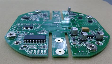
Printed Circuit Boards (PCBs) are the backbone of modern electronic devices, serving as the platform upon which electronic components are mounted and interconnected. A critical aspect of PCB design and functionality is the wiring, which ensures that electrical signals and power are efficiently distributed across the board. Understanding the basics of PCB wire connections is essential for anyone involved in electronics design or manufacturing, as it directly impacts the performance and reliability of the final product.
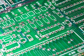
To begin with, PCB wire connections are typically established through traces, which are thin lines of conductive material, usually copper, etched onto the board.
These traces act as the pathways for electrical signals, connecting various components such as resistors, capacitors, and integrated circuits. The design of these traces is crucial, as their width, thickness, and length can affect the board’s electrical characteristics, including resistance, capacitance, and inductance. Therefore, careful consideration must be given to the trace layout during the PCB design process to ensure optimal performance.
In addition to traces, vias are another important element of PCB wire connections.
Vias are small holes drilled through the board that allow traces to connect between different layers of a multi-layer PCB. This vertical interconnection is vital for complex circuits where space is limited, and multiple layers are necessary to accommodate all the required connections. Vias can be classified into different types, such as through-hole vias, blind vias, and buried vias, each serving specific purposes depending on the design requirements.
Moreover, the choice of materials for PCB wire connections plays a significant role in the board’s overall performance.
Copper is the most commonly used material for traces due to its excellent conductivity and relatively low cost. However, in high-frequency applications, where signal integrity is paramount, alternative materials such as gold or silver may be used to reduce signal loss and improve performance. Additionally, the substrate material, typically made of fiberglass-reinforced epoxy resin, must be carefully selected to provide the necessary mechanical support and thermal stability.
Another critical aspect of PCB wire connections is the soldering process, which is used to attach components to the board.
Soldering involves melting a metal alloy, usually composed of tin and lead or lead-free alternatives, to create a strong electrical and mechanical bond between the component leads and the PCB pads. Proper soldering techniques are essential to prevent issues such as cold joints, which can lead to intermittent connections and device failure. Furthermore, advancements in soldering technology, such as surface mount technology (SMT), have enabled the production of smaller and more densely packed PCBs, further emphasizing the importance of precise wire connections.
In conclusion, understanding the basics of PCB wire connections is fundamental for ensuring the functionality and reliability of electronic devices. From the design of traces and vias to the selection of materials and soldering techniques, each aspect plays a crucial role in the overall performance of the PCB. As technology continues to advance, the demand for more complex and efficient PCB designs will only increase, making a solid grasp of these principles more important than ever for professionals in the electronics industry. By mastering these foundational concepts, designers and engineers can create PCBs that meet the ever-growing demands of modern technology.
Innovations In PCB Wire Design For Enhanced Performance
Printed Circuit Boards (PCBs) are the backbone of modern electronic devices, serving as the foundation upon which electronic components are mounted and interconnected. As technology continues to advance, the demand for more efficient, reliable, and compact electronic devices has driven innovations in PCB wire design. These innovations are crucial for enhancing the performance of electronic systems, ensuring they meet the ever-increasing expectations of both consumers and industries.
One of the primary areas of innovation in PCB wire design is the development of advanced materials.
Traditional copper wires, while effective, are being supplemented or replaced by materials that offer superior conductivity and thermal management. For instance, the use of silver and gold in certain applications, despite their higher cost, can significantly reduce resistance and improve signal integrity. Additionally, the incorporation of graphene and other nanomaterials is being explored for their exceptional electrical properties and potential to revolutionize PCB wire design.
Moreover, the miniaturization of electronic components has necessitated the development of finer and more precise wire designs.
As devices become smaller, the space available for wiring decreases, requiring engineers to innovate in terms of wire thickness and layout. Techniques such as microvia technology, which involves creating extremely small vias to connect different layers of a PCB, have become increasingly important. This technology not only saves space but also enhances the electrical performance by reducing the length of the conductive path.
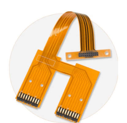
In addition to material and size innovations, the integration of flexible PCB wires is gaining traction.
Flexible PCBs, which can bend and fold without breaking, are ideal for applications where space is constrained or where the PCB must conform to a specific shape. This flexibility is particularly beneficial in wearable technology, medical devices, and automotive applications, where traditional rigid PCBs would be impractical. The design of flexible PCB wires involves careful consideration of materials and manufacturing processes to ensure durability and reliability under repeated flexing.
Furthermore, the rise of high-frequency applications, such as 5G technology and advanced computing, has spurred innovations in PCB wire design to address issues related to signal integrity and electromagnetic interference (EMI).
Engineers are developing specialized wire geometries and shielding techniques to minimize signal loss and crosstalk, thereby ensuring that high-speed data can be transmitted accurately and efficiently. These innovations are critical for maintaining the performance of devices operating at gigahertz frequencies and beyond.
Another significant trend in PCB wire design is the emphasis on sustainability and environmental impact.
As electronic waste becomes a growing concern, there is a push towards using eco-friendly materials and manufacturing processes. Innovations in biodegradable and recyclable PCB materials are being explored, alongside methods to reduce the energy consumption of PCB production. These efforts not only contribute to environmental conservation but also align with the increasing consumer demand for sustainable products.
In conclusion, the field of PCB wire design is undergoing rapid transformation driven by the need for enhanced performance in modern electronic devices. Through advancements in materials, miniaturization techniques, flexible designs, high-frequency capabilities, and sustainable practices, engineers are pushing the boundaries of what is possible in electronic design. As these innovations continue to evolve, they will undoubtedly play a pivotal role in shaping the future of technology, enabling the development of more powerful, efficient, and environmentally friendly electronic systems.

Common Challenges In PCB Wire Assembly And How To Overcome Them
Printed Circuit Board (PCB) wire assembly is a critical component in the manufacturing of electronic devices, serving as the backbone for electrical connectivity. However, this process is fraught with challenges that can impact the performance and reliability of the final product. Understanding these challenges and implementing strategies to overcome them is essential for manufacturers aiming to produce high-quality electronic devices.
One of the primary challenges in PCB wire assembly is ensuring precise wire routing.
As electronic devices become more compact, the available space for wire routing diminishes, making it increasingly difficult to avoid interference and maintain signal integrity. To address this, manufacturers can employ advanced computer-aided design (CAD) software that allows for meticulous planning of wire paths. This software can simulate various routing scenarios, helping engineers identify potential issues before the physical assembly begins. Additionally, using multi-layer PCBs can provide more routing options, thereby reducing congestion and minimizing the risk of crosstalk between wires.
Another significant challenge is the selection of appropriate wire materials.
The choice of wire material can greatly influence the performance, durability, and cost of the PCB assembly. Copper is commonly used due to its excellent conductivity and flexibility, but it may not always be the best choice for high-frequency applications where signal loss is a concern. In such cases, manufacturers might consider using silver-plated or gold-plated wires, which offer superior conductivity and resistance to oxidation. However, these materials come at a higher cost, necessitating a careful cost-benefit analysis to ensure that the performance gains justify the additional expense.
Soldering is another critical aspect of PCB wire assembly that presents its own set of challenges.
Achieving a reliable solder joint is essential for ensuring electrical connectivity and mechanical stability. Poor soldering can lead to issues such as cold joints, bridging, and voids, which can compromise the functionality of the PCB. To mitigate these risks, manufacturers should invest in high-quality soldering equipment and ensure that their technicians are well-trained in soldering techniques. Additionally, implementing rigorous quality control measures, such as X-ray inspection and automated optical inspection (AOI), can help identify and rectify soldering defects before the PCB is deployed.
Thermal management is also a crucial consideration in PCB wire assembly.
As electronic devices operate, they generate heat, which can degrade the performance of the PCB and lead to premature failure. Effective thermal management involves selecting materials with good thermal conductivity, designing PCBs with adequate heat dissipation features, and incorporating components such as heat sinks and thermal vias. By addressing thermal challenges early in the design process, manufacturers can enhance the reliability and longevity of their products.
Finally, maintaining compliance with industry standards and regulations is a challenge that cannot be overlooked.
Standards such as IPC-A-610 and IPC/WHMA-A-620 provide guidelines for the acceptability of electronic assemblies and wire harnesses, respectively. Adhering to these standards ensures that PCB wire assemblies meet the necessary quality and safety requirements. Manufacturers should stay informed about updates to these standards and invest in training programs to ensure that their workforce is knowledgeable about compliance requirements.
In conclusion, while PCB wire assembly presents several challenges, they can be effectively managed through careful planning, material selection, and adherence to industry standards. By leveraging advanced technologies and maintaining a focus on quality, manufacturers can overcome these obstacles and produce reliable, high-performance electronic devices.
The Role Of PCB Wire In Modern Electronics Manufacturing
In the rapidly evolving landscape of modern electronics manufacturing, the role of printed circuit board (PCB) wire is both pivotal and multifaceted. As the backbone of electronic devices, PCBs serve as the foundation upon which components are mounted and interconnected. The integration of PCB wire into these systems is crucial for ensuring the seamless transmission of electrical signals, thereby enabling the functionality of a wide array of electronic products. To appreciate the significance of PCB wire, it is essential to understand its contribution to the efficiency, reliability, and miniaturization of electronic devices.
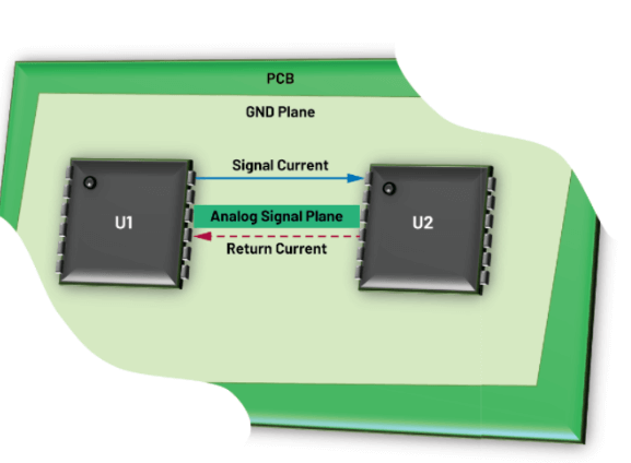
PCB wire, often referred to as wire harnesses or jumpers, is employed to establish connections between different points on a circuit board.
This is particularly important in complex circuits where multiple layers and components are involved. By facilitating these connections, PCB wire ensures that electrical signals can travel unimpeded across the board, thereby maintaining the integrity of the circuit’s operation. Moreover, the use of high-quality PCB wire can significantly reduce the risk of signal loss or interference, which is critical in applications where precision and reliability are paramount.
In addition to its role in signal transmission, PCB wire also contributes to the structural integrity of electronic devices.
As electronic products become increasingly compact, the demand for miniaturization has led to the development of more intricate circuit designs. PCB wire plays a crucial role in this context by allowing for the efficient use of space within the device. By enabling connections that would otherwise require additional board space, PCB wire helps manufacturers achieve the desired form factor without compromising on performance. This is particularly evident in consumer electronics, where sleek and compact designs are highly sought after.
Furthermore, the versatility of PCB wire makes it an indispensable component in the manufacturing process.
It can be customized to meet specific requirements, such as varying lengths, insulation types, and conductor materials. This adaptability allows manufacturers to tailor PCB wire to suit the unique demands of different applications, ranging from consumer electronics to industrial machinery. As a result, PCB wire is not only a critical component in the assembly of electronic devices but also a key factor in their overall design and functionality.
The importance of PCB wire is further underscored by its role in enhancing the durability and longevity of electronic products.
By providing robust connections that can withstand mechanical stress and environmental factors, PCB wire helps ensure that devices remain operational over extended periods. This is particularly important in industries where reliability is non-negotiable, such as aerospace and medical technology. In these sectors, the failure of a single connection can have far-reaching consequences, making the quality and reliability of PCB wire a top priority.
In conclusion, the role of PCB wire in modern electronics manufacturing is both comprehensive and indispensable. By facilitating efficient signal transmission, contributing to miniaturization, and enhancing the durability of electronic devices, PCB wire plays a critical role in the advancement of technology. As the demand for more sophisticated and reliable electronic products continues to grow, the importance of PCB wire in the manufacturing process is likely to increase, underscoring its status as a fundamental component in the world of electronics.