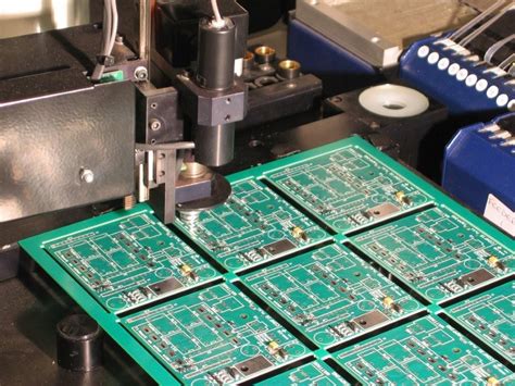
PCB wiring skills to reduce signal coupling during RF product design
A wave of demand for Bluetooth devices, cordless phones and cellular phones is prompting Chinese electronic engineers to pay more and more attention to RF circuit design skills. The design of RF circuit boards is the most troublesome part for design engineers. If you want to succeed at the first time, careful planning and attention to details are two key design rules that must be highly valued.
Radio frequency (RF) circuit board design is often described as a “black art” because there are still many uncertainties in theory, but this view is only partially correct. There are also many rules that can be followed and laws that should not be ignored in RF circuit board design. However, in actual design, the real practical skill is how to compromise these rules and laws when they cannot be accurately implemented due to various design constraints.
Of course, there are many important RF design topics worth discussing, including impedance and impedance matching, dielectric layer materials and laminates, and wavelengths and standing waves.
However, this article will focus on various issues related to RF circuit board partition design.
Today’s cellular phone designs integrate everything together in various ways, which is not good for RF circuit board design. The industry is very competitive now, and everyone is looking for ways to integrate the most functions with the smallest size and the lowest cost. Analog, digital and RF circuits are all tightly packed together, with very little space to separate their respective problem areas, and considering cost factors, the number of circuit board layers is often minimized.
Incredibly, multi-purpose chips can integrate multiple functions on a very small die, and the pins connecting to the outside world are arranged very closely, so RF, IF, analog and digital signals are very close, but they are usually electrically unrelated. Power distribution can be a nightmare for designers. In order to extend battery life, different parts of the circuit are time-sharing as needed, and the conversion is controlled by software. This means that you may need to provide 5 to 6 working power supplies for your cell phone.
1.RF layout concept
When designing RF layout, there are several general principles that must be met first:
I
solate the high-power RF amplifier (HPA) and the low-noise amplifier (LNA) as much as possible. Simply put, keep the high-power RF transmission circuit away from the low-power RF receiving circuit. If you have a lot of physical space on your PCB board, you can easily do this, but usually there are many components and the PCB space is small, so this is usually impossible. You can put them on both sides of the PCB board, or let them work alternately instead of working at the same time. High-power circuits sometimes also include RF buffers and voltage-controlled oscillators (VCOs).
Make sure that there is at least one whole ground in the high-power area of the PCB board, preferably without vias on it.
Of course, the more copper the better. Later, we will discuss how to break this design principle as needed and how to avoid the problems that may arise from it.
Chip and power supply decoupling is also extremely important, and several methods to implement this principle will be discussed later.
RF outputs usually need to be kept away from RF inputs, which we will discuss in detail later.
Sensitive analog signals should be as far away from high-speed digital signals and RF signals as possible.
2.How to partition?
Design partitions can be decomposed into physical partitions and electrical partitions. Physical partitions mainly involve issues such as component layout, orientation and shielding; electrical partitions can be further decomposed into partitions for power distribution, RF routing, sensitive circuits and signals, and grounding.
First, let’s discuss the issue of physical partitions.
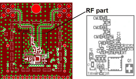
Component layout is the key to achieving an excellent RF design. The most effective technique is to first fix the components on the RF path and adjust their orientation to minimize the length of the RF path, keep the input away from the output, and separate the high-power circuit and the low-power circuit as far as possible.
The most effective circuit board stacking method is to arrange the main ground plane (main ground) on the second layer under the surface layer and run the RF line on the surface layer as much as possible. Minimizing the size of the vias on the RF path can not only reduce the path inductance, but also reduce the number of cold solder joints on the main ground and reduce the chance of RF energy leaking to other areas in the stacked board.
In physical space, linear circuits such as multi-stage amplifiers are usually sufficient to isolate multiple RF areas from each other, but duplexers, mixers, and intermediate frequency amplifiers/mixers always have multiple RF/IF signals interfering with each other, so this effect must be carefully minimized. RF and IF traces should be crossed as much as possible, and a ground should be placed between them as much as possible. The correct RF path is very important for the performance of the entire PCB board, which is why component layout usually takes up most of the time in the design of cellular phone PCB boards.
On cellular phone PCB boards, the low noise amplifier circuit can usually be placed on one side of the PCB board, and the high power amplifier on the other side, and finally connected to the antenna on the RF side and the baseband processor side on the same side through a duplexer. Some skills are needed to ensure that the straight through hole does not transfer RF energy from one side of the board to the other side. A common technique is to use blind holes on both sides. The adverse effects of straight through holes can be minimized by arranging the straight through holes in areas that are not affected by RF interference on both sides of the PCB board.
Sometimes it is not possible to ensure sufficient isolation between multiple circuit blocks. In this case, it is necessary to consider using a metal shield to shield the RF energy in the RF area. However, metal shields also have problems, such as: the cost of the shield itself and the assembly cost are very high;
It is difficult to ensure high precision when manufacturing irregular metal shields, and rectangular or square metal shields restrict the layout of components; metal shields are not conducive to component replacement and fault location; because metal shields must be soldered to the ground, they must be kept at an appropriate distance from the components, so they need to occupy valuable PCB board space.

It is very important to ensure the integrity of the shield as much as possible.
The digital signal line entering the metal shield should be routed on the inner layer as much as possible, and it is best that the PCB layer below the routing layer is the ground layer. The RF signal line can go out from the small gap at the bottom of the metal shield and the wiring layer at the ground gap, but as much ground as possible should be laid around the gap, and the ground on different layers can be connected together through multiple vias.
Despite the above problems, metal shields are very effective and are often the only solution to isolate critical circuits.
In addition, proper and effective chip power decoupling is also very important. Many RF chips with integrated linear circuits are very sensitive to power supply noise. Usually, each chip needs to use up to four capacitors and one isolation inductor to ensure that all power supply noise is filtered out (see Figure 1).
The minimum capacitor value is usually determined by its self-resonant frequency and low pin inductance, and the value of C4 is selected accordingly. The values of C3 and C2 are relatively large due to their own pin inductance, so the RF decoupling effect is poor, but they are more suitable for filtering lower frequency noise signals.
Inductor L1 prevents RF signals from coupling from the power line into the chip.
Remember: all traces are potential antennas that can both receive and transmit RF signals. In addition, it is also necessary to isolate the induced RF signals from critical lines. The physical location of these decoupling components is usually also critical. Figure 2 shows a typical layout method.
The layout principles of these important components are: C4 should be as close to the IC pin as possible and grounded, C3 must be closest to C4, C2 must be closest to C3, and the connection traces between the IC pin and C4 should be as short as possible.
The ground ends of these components (especially C4) should usually be connected to the ground pin of the chip through the next layer.
The vias connecting the components to the ground plane should be as close as possible to the component pads on the PCB board. It is best to use blind holes punched on the pads to minimize the inductance of the connection line. The inductor should be close to C1.
An integrated circuit or amplifier often has an open-drain output, so a pull-up inductor is required to provide a high-impedance RF load and a low-impedance DC power supply. The same principle applies to decoupling the power supply at the end of this inductor.
Some chips require multiple power supplies to work, so you may need two or three sets of capacitors and inductors to decouple them separately. If there is not enough space around the chip, you may encounter some trouble.
Remember that inductors are rarely placed in parallel, because this will form an air-core transformer and induce interference signals to each other, so the distance between them should be at least equivalent to the height of one of the components, or arranged at right angles to minimize their mutual inductance.
The principles of electrical partitioning are generally the same as physical partitioning, but there are also some other factors.
Some parts of modern cellular phones use different operating voltages and are controlled by software to extend battery life. This means that cellular phones need to run multiple power supplies, which brings more problems to isolation. Power is usually introduced from the connector and immediately decoupled to filter out any noise from outside the circuit board before being distributed through a set of switches or regulators.
Most of the circuits in a cell phone have very low DC currents, so trace width is usually not an issue, but the power supply of the high-power amplifier must be routed as wide as possible to minimize the transmission voltage drop. To avoid too much current loss, multiple vias are needed to pass the current from one layer to another. In addition, if the power supply pin of the high-power amplifier is not adequately decoupled, high-power noise will radiate throughout the board and cause various problems.
The grounding of the high-power amplifier is quite critical and often requires a metal shielding can.
In most cases, it is also critical to ensure that the RF output is kept away from the RF input. This also applies to amplifiers, buffers, and filters. In the worst case, if the outputs of amplifiers and buffers are fed back to their inputs with appropriate phase and amplitude, they may produce self-oscillation. In the best case, they will be stable under all temperature and voltage conditions. In fact, they may become unstable and add noise and intermodulation signals to the RF signal.
If the RF signal line has to loop back from the input of the filter to the output, this may seriously degrade the filter’s passband characteristics. In order to achieve good isolation between the input and output, first a ring of ground must be laid around the filter, and then a ground must be laid in the lower area of the filter and connected to the main ground around the filter. It is also a good idea to keep the signal lines that need to pass through the filter as far away from the filter pins as possible.
In addition, grounding should be done very carefully in various places throughout the board, otherwise you may unknowingly introduce an unwanted coupling path. Figure 3 details this grounding method.
Sometimes you can choose to run single-ended or balanced RF signal lines. The same principles about crosstalk and EMC/EMI apply here. Balanced RF signal lines can reduce noise and crosstalk if they are routed correctly, but their impedance is usually higher, and it may be difficult to maintain a reasonable line width to obtain an impedance matching the signal source, line and load.
Buffers can be used to improve isolation because they can split the same signal into two parts and use them to drive different circuits.
In particular, the local oscillator may need a buffer to drive multiple mixers. When a mixer reaches common-mode isolation at RF frequencies, it will not work properly. Buffers are a great way to isolate impedance changes at different frequencies so that circuits do not interfere with each other.
Buffers are very helpful in design because they can be placed right after the circuits they need to drive, making high-power output traces very short, and because the input signal level of the buffers is relatively low, they are less likely to interfere with other circuits on the board.
There are many very sensitive signal and control lines that require special attention, but they are beyond the scope of this article, so they are only briefly discussed and not explained in detail.
Voltage-controlled oscillators (VCOs) convert varying voltages into varying frequencies, which is used for high-speed channel switching, but they also convert tiny amounts of noise on the control voltage into tiny frequency changes, which adds noise to the RF signal. In general, you can no longer remove noise from the RF output signal after this stage.
So what’s the problem?
First, the desired bandwidth of the control line may range from DC to 2MHz, and it is almost impossible to remove such a wide bandwidth of noise by filtering; second, the VCO control line is usually part of a feedback loop that controls the frequency, which may introduce noise in many places, so the VCO control line must be handled very carefully.
Make sure that the ground under the RF trace is solid, and all components are firmly connected to the main ground and isolated from other traces that may bring noise. In addition, make sure that the power supply of the VCO has been fully decoupled. Since the RF output of the VCO is often a relatively high level, the VCO output signal can easily interfere with other circuits, so special attention must be paid to the VCO. In fact, the VCO is often placed at the end of the RF area, and sometimes it also requires a metal shield.
The resonant circuit (one for the transmitter and the other for the receiver) is related to the VCO, but it also has its own characteristics. Simply put, the resonant circuit is a parallel resonant circuit with a capacitive diode, which helps set the VCO operating frequency and modulate voice or data onto the RF signal.
All VCO design principles also apply to the resonant circuit. Resonant circuits are often very sensitive to noise because they contain a relatively large number of components, have a wide distribution area on the board, and usually operate at a very high RF frequency.
Signals are usually arranged on adjacent pins of the chip, but these signal pins need to work with relatively large inductors and capacitors, which in turn require that these inductors and capacitors be located very close together and connected back to a control loop that is very sensitive to noise. This is not easy to achieve.
Automatic gain control (AGC) amplifiers are also prone to problems. AGC amplifiers are present in both transmit and receive circuits.
AGC amplifiers are usually effective in filtering noise, but the ability of cellular phones to handle rapid changes in transmit and receive signal strength requires a relatively wide bandwidth, which makes the AGC amplifiers on certain critical circuits very susceptible to noise.
Designing AGC circuits must follow good analog circuit design techniques, which are related to very short op amp input pins and very short feedback paths, both of which must be far away from RF, IF or high-speed digital signal traces. Likewise, good grounding is essential, and the chip’s power supply must be well decoupled. If you must run a long line at the input or output, it is best to run it at the output, which usually has much lower impedance and is less likely to pick up noise. Usually the higher the signal level, the easier it is to pick up noise
The sound is introduced into other circuits.
In all PCB designs, it is a general principle to keep digital circuits away from analog circuits as much as possible, and it also applies to RF PCB design. Common analog ground and ground used for shielding and separating signal lines are usually equally important.
The problem is that if there is no foresight and careful planning in advance, there is little you can do in this regard every time.
Therefore, careful planning, thoughtful component layout and thorough layout evaluation are very important in the early stages of design. Design changes caused by negligence may cause a nearly completed design to be torn down and re-started. This serious consequence caused by negligence is not a good thing for your personal career development anyway.
RF lines should also be kept away from analog lines and some very critical digital signals.
All RF traces, pads and components should be filled with ground copper as much as possible and connected to the main ground as much as possible. Micro-via construction boards similar to breadboards are very useful in the RF circuit development stage. If you choose a construction board, you can use many vias at will without any cost. Otherwise, drilling holes on ordinary PCB boards will increase
development costs, which will increase costs in mass production.
If RF traces must cross signal lines, try to place a ground plane between them and along the RF traces that is connected to the main ground.
If this is not possible, make sure they are crisscrossed, which minimizes capacitive coupling, and place as much ground as possible around each RF trace and connect them to the main ground. In addition, minimize the distance between parallel RF traces to minimize inductive coupling.
A solid, monolithic ground plane is best placed on the first layer directly below the surface layer for isolation, although other approaches can work with careful design.
I have tried to separate analog, digital, and RF lines by splitting the ground plane into several pieces, but I have never been satisfied with the results because there are always some high-speed signal lines that need to pass through these separate grounds, which is not a good thing.
On each layer of the PCB, you should place as many ground planes as possible and connect them to the main ground.
Put traces together as much as possible to increase the number of land plots on internal signal layers and power distribution layers, and adjust the traces appropriately so that you can place ground connection vias to the isolated land plots on the surface layer. Avoid creating stray grounds on PCB layers because they can pick up or inject noise like a small antenna. In most cases, if you can’t connect them to the main ground, then you’d better remove them.
Summary
When you get an engineering change order (ECO), stay calm and don’t easily eliminate all your hard work. An ECO can easily throw your work into chaos, no matter how small the changes required are. When you have to complete a job in a certain period of time, it’s easy to forget something critical, let alone make changes.
Whether it’s a “black art” or not, following some basic RF design rules and paying attention to some good design examples will help you complete RF design work. Successful RF design can only be achieved by paying careful attention to every step and every detail of the entire design process, which means that thorough and careful planning must be carried out at the beginning of the design, and comprehensive and continuous evaluation of the progress of each design step.