Pcba board
Differences Between PCB and PCBA board: A Comprehensive Guide
Printed Circuit Boards (PCBs) and Printed Circuit Board Assemblies (PCBAs) are fundamental components in the electronics industry, yet they serve distinct roles and possess unique characteristics. Understanding the differences between PCB and PCBA is crucial for anyone involved in electronics design, manufacturing, or repair. This comprehensive guide aims to elucidate these differences, providing clarity on their respective functions, processes, and applications.
At the most basic level, a PCB is a flat board made of non-conductive material, typically fiberglass, that serves as a foundation for electronic components.
The board itself is etched with conductive pathways, or traces, made of copper, which facilitate the flow of electrical signals between components. These traces are meticulously designed to ensure optimal performance and reliability. PCBs come in various types, including single-sided, double-sided, and multi-layered boards, each offering different levels of complexity and functionality.
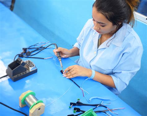
In contrast, a PCBA refers to a PCB that has undergone the assembly process, where electronic components such as resistors, capacitors, and integrated circuits are mounted onto the board. This transformation from a bare PCB to a fully functional PCBA involves several steps, including soldering, inspection, and testing. The assembly process can be executed using either Surface Mount Technology (SMT) or Through-Hole Technology (THT), depending on the design requirements and the nature of the components involved.
One of the primary differences between PCB and PCBA lies in their respective stages within the electronics manufacturing lifecycle.
A PCB is essentially the blank canvas, providing the necessary infrastructure for electronic circuits. It is during the PCBA stage that the board becomes operational, as components are added and interconnected to perform specific functions. This distinction is critical, as it underscores the transition from a passive structure to an active, functional assembly.
Moreover, the complexity and cost associated with PCBs and PCBAs vary significantly.
The fabrication of a PCB involves precise engineering and manufacturing techniques to create the intricate network of traces. Factors such as the number of layers, trace width, and spacing can influence the complexity and cost of the PCB. On the other hand, the assembly process for a PCBA introduces additional variables, including component sourcing, placement accuracy, and soldering quality. Consequently, PCBAs tend to be more expensive than bare PCBs due to the added labor, materials, and quality control measures required.
Another key difference pertains to the testing and quality assurance processes.
While PCBs undergo electrical testing to verify the integrity of the traces and connections, PCBAs require more comprehensive testing to ensure that the assembled components function correctly. This may involve in-circuit testing (ICT), functional testing, and even environmental stress testing to validate the performance and reliability of the final product.
In terms of applications, PCBs are ubiquitous in virtually all electronic devices, serving as the backbone for circuits in everything from simple gadgets to complex systems.
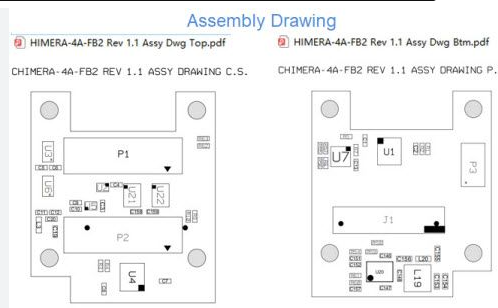
PCBAs, however, are the end products that power these devices, enabling them to perform their intended functions. For instance, a smartphone’s motherboard is a PCBA that integrates various components to manage processing, communication, and power distribution.
In conclusion, while PCBs and PCBAs are intrinsically linked, they represent different stages and aspects of electronic manufacturing. A PCB provides the structural and electrical foundation, whereas a PCBA transforms this foundation into a functional entity through the addition of electronic components. Recognizing these differences is essential for professionals in the electronics industry, as it informs decisions related to design, manufacturing, and quality assurance.
PCB vs PCBA: Which One Do You Need for Your Project?
When embarking on an electronics project, understanding the distinction between a Printed Circuit Board (PCB) and a Printed Circuit Board Assembly (PCBA) is crucial. Both components play integral roles in the development and functionality of electronic devices, yet they serve different purposes and are utilized at different stages of the manufacturing process. To determine which one you need for your project, it is essential to comprehend their definitions, functions, and applications.
A Printed Circuit Board (PCB) is essentially the skeletal framework of an electronic device.
It consists of a flat, insulating substrate, typically made of fiberglass, upon which conductive pathways are etched or printed. These pathways, often referred to as traces, facilitate the electrical connections between various components. PCBs can be single-sided, double-sided, or multi-layered, depending on the complexity and requirements of the electronic device. The primary function of a PCB is to provide a stable and organized platform for mounting electronic components, ensuring that electrical signals are transmitted efficiently and reliably.
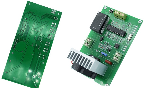
On the other hand, a Printed Circuit Board Assembly (PCBA) refers to a PCB that has been populated with electronic components.
This process involves soldering components such as resistors, capacitors, integrated circuits, and connectors onto the PCB. The assembly process can be performed manually or through automated machinery, depending on the scale and precision required. A PCBA is essentially a functional electronic circuit, ready to be integrated into a larger system or device. It is the culmination of the design and manufacturing process, transforming a bare PCB into a working electronic assembly.
To determine whether you need a PCB or a PCBA for your project, it is important to consider the stage of development you are in.
If you are in the initial design phase, focusing on the layout and routing of electrical connections, a PCB is what you require. During this phase, you will work on creating the schematic diagram, selecting the appropriate materials, and designing the board layout. Once the design is finalized, the PCB can be fabricated, providing you with the physical board that will serve as the foundation for your electronic device.
However, if you have already completed the design phase and are ready to bring your project to life, a PCBA is what you need.
This involves procuring the necessary components and assembling them onto the PCB. The assembly process requires precision and expertise to ensure that all components are correctly placed and soldered, minimizing the risk of defects and ensuring optimal performance. A PCBA is essentially the final product that can be tested, validated, and integrated into your electronic device.
In conclusion, the choice between a PCB and a PCBA depends on the specific stage of your project. A PCB is essential during the design and layout phase, providing the structural foundation for your electronic device. Conversely, a PCBA is required during the assembly phase, transforming the bare PCB into a functional electronic circuit. Understanding the roles and applications of both components will enable you to make informed decisions, ensuring the successful development and implementation of your electronics project. By recognizing the distinct functions of PCBs and PCBAs, you can streamline your workflow, optimize your resources, and achieve your project goals efficiently.
The Manufacturing Process: PCB vs PCBA
The manufacturing process of Printed Circuit Boards (PCBs) and Printed Circuit Board Assemblies (PCBAs) involves a series of intricate steps, each critical to the final product’s functionality and reliability. Understanding the distinctions between these two processes is essential for anyone involved in electronics manufacturing or design.
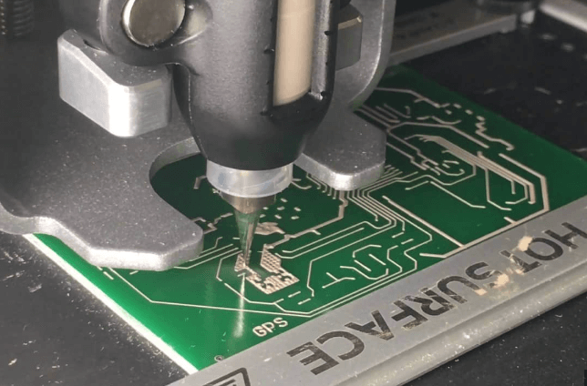
Initially, the creation of a PCB begins with the design phase, where engineers use specialized software to draft the circuit layout.
This layout is then transferred onto a substrate, typically made of fiberglass or other insulating materials. The substrate is coated with a thin layer of conductive material, usually copper, which is then etched away to leave behind the desired circuit pattern. This etching process can be achieved through various methods, such as chemical etching or laser etching, each offering different levels of precision and cost-effectiveness.
Following the etching process, the PCB undergoes a series of inspections to ensure that the circuit paths are correctly formed and free of defects.
These inspections may include visual checks, automated optical inspections (AOI), and electrical testing. Once the PCB passes these quality control measures, it is ready for the next stage: drilling. Holes are drilled into the board to accommodate components and vias, which are conductive pathways that allow electrical connections between different layers of the PCB.
After drilling, the PCB is cleaned to remove any debris or contaminants that could affect its performance.
The board is then plated with additional layers of copper to reinforce the circuit paths and improve conductivity. This plating process is followed by the application of a solder mask, which protects the copper traces from oxidation and prevents solder bridges during component placement. The final step in PCB manufacturing is the application of a silkscreen layer, which provides labels and markings to assist in component placement and troubleshooting.
Transitioning from PCB to PCBA, the focus shifts from the board itself to the assembly of components onto the board.
The PCBA process begins with the application of solder paste to the PCB. This paste, composed of tiny solder balls suspended in flux, is applied to the areas where components will be mounted. The PCB then moves to a pick-and-place machine, which accurately positions components onto the board based on the design specifications.
Once all components are in place, the PCB undergoes a reflow soldering process.
During reflow soldering, the board is heated in a controlled environment, causing the solder paste to melt and form solid connections between the components and the PCB. This step is crucial for ensuring that all components are securely attached and electrically connected.
Following reflow soldering, the PCBA is subjected to a series of inspections and tests to verify its functionality.
These may include AOI, X-ray inspection, and in-circuit testing (ICT). Any defects identified during these inspections are addressed through rework processes, which may involve manual soldering or component replacement.
In conclusion, while the manufacturing processes of PCBs and PCBAs share some similarities, they are distinct in their focus and execution. The PCB process is primarily concerned with creating the physical board and its circuit paths, whereas the PCBA process involves the assembly and testing of components on the board.
Both processes require meticulous attention to detail and rigorous quality control to ensure the final product meets the required specifications and performance standards. Understanding these processes is fundamental for anyone involved in the electronics industry, as it provides insight into the complexities and challenges of modern electronics manufacturing.
Cost Comparison: PCB vs PCBA
When evaluating the cost implications of Printed Circuit Boards (PCBs) versus Printed Circuit Board Assemblies (PCBAs), it is essential to understand the distinct stages of production and the factors influencing their respective expenses. A PCB, in its simplest form, is a bare board that serves as the foundation for electronic components. In contrast, a PCBA is a fully assembled board, complete with all necessary components soldered onto the PCB. The cost comparison between these two entities involves a multifaceted analysis of material costs, manufacturing processes, labor, and additional overheads.
To begin with, the cost of a PCB is primarily determined by the materials used and the complexity of the board design.
PCBs are typically made from fiberglass-reinforced epoxy laminate sheets, with copper foil laminated on one or both sides. The number of layers, board thickness, and the intricacy of the circuit design can significantly impact the cost. For instance, a simple single-layer PCB will be less expensive than a multi-layer board with intricate routing and fine pitch components. Additionally, specialized materials such as high-frequency laminates or flexible substrates can further escalate the cost.
Transitioning to PCBAs, the cost structure becomes more complex due to the inclusion of electronic components and the assembly process.
The price of components can vary widely based on their type, quality, and sourcing. High-performance or specialized components, such as microprocessors or custom integrated circuits, can be particularly costly. Furthermore, the global supply chain dynamics, including component availability and lead times, can influence prices. For example, shortages of specific components can drive up costs due to increased demand and limited supply.
The assembly process itself introduces additional costs.
Surface Mount Technology (SMT) and Through-Hole Technology (THT) are the two primary methods used to assemble components onto PCBs. SMT is generally more cost-effective for high-volume production runs due to its automation capabilities, whereas THT may be preferred for components that require stronger mechanical bonds or for low-volume, specialized applications. The choice of assembly method can thus impact the overall cost of a PCBA.
Labor costs also play a significant role in the cost comparison between PCBs and PCBAs.
While PCB manufacturing is largely automated, reducing the need for manual intervention, the assembly process for PCBAs often requires skilled labor, especially for quality control and testing. The geographical location of the manufacturing facility can further influence labor costs, with regions having lower labor rates potentially offering cost advantages.
Moreover, additional overheads such as testing, quality assurance, and compliance with industry standards can add to the cost of PCBAs.
Rigorous testing procedures, including in-circuit testing (ICT) and functional testing, are essential to ensure the reliability and performance of the assembled boards. Compliance with standards such as IPC-A-610 for electronic assemblies or ISO 9001 for quality management systems can also incur additional costs but are crucial for maintaining product quality and customer satisfaction.
In conclusion, while the initial cost of a bare PCB may be relatively low, the transition to a fully assembled PCBA introduces a range of additional expenses related to components, assembly processes, labor, and quality assurance. Therefore, when comparing the costs of PCBs versus PCBAs, it is important to consider the entire production lifecycle and the various factors that contribute to the final cost. This comprehensive understanding enables more informed decision-making and effective cost management in the production of electronic devices.