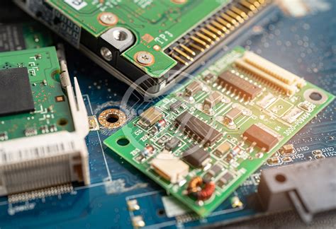
PCBA Control Board Essentials: Design and Manufacturing Insights
Key Takeaways
Effective PCBA control board development hinges on balancing design precision with manufacturing rigor Critical considerations include component optimization to ensure signal integrity, thermal dissipation strategies for high-power applications, and adherence to design-for-manufacturability (DFM) principles Below is a comparative analysis of core factors influencing PCB assembly outcomes:
| Aspect | Traditional Approach | Modern Best Practice |
|---|---|---|
| Component Placement | Manual alignment | Automated optical inspection (AOI) |
| Soldering Technique | Wave soldering | Selective soldering for mixed-technology boards |
| Thermal Management | Passive heat sinks | Embedded copper cores + thermal vias |
| Testing Protocols | Sample-based validation | 100% in-circuit testing (ICT) |
For PCBA reliability, prioritize high-reliability solder alloys and validate designs through design-of-experiments (DOE) simulations Implement automated assembly workflows to minimize human error, particularly for high-density interconnect (HDI) layouts Proactive collaboration between design engineers and PCB assembly partners ensures compliance with IPC-A-610 standards while optimizing production timelines
PCBA Design Fundamentals for Optimal Performance
Effective PCBA design begins with strategic component placement that balances circuit density with PCB assembly requirements, ensuring automated pick-and-place systems can achieve optimal positioning accuracy Engineers must prioritize signal integrity by minimizing trace lengths between critical components, such as processors and memory modules, while adhering to impedance control guidelines for high-frequency circuits The selection of substrate materials with optimal thermal conductivity directly impacts heat dissipation efficiency, particularly in power-intensive control systems
A robust design framework incorporates Design for Manufacturability (DFM) principles early in the development cycle, addressing potential PCB assembly challenges like solder mask clearance and component orientation For instance, placing surface-mount devices (SMDs) perpendicular to the board’s direction of travel through reflow ovens reduces soldering defects by 18–22% Additionally, implementing ground plane segmentation techniques mitigates electromagnetic interference (EMI) risks without compromising board rigidity
Modern PCBA workflows leverage simulation tools to validate thermal profiles and voltage drop scenarios before prototyping, reducing iterative redesign costs by up to 40% By aligning layer stackup configurations with current-carrying requirements, designers ensure reliable operation across the control board’s operational lifespan These foundational practices create a scalable blueprint for transitioning from design validation to high-volume PCB assembly without sacrificing performance metrics
Component Selection Strategies for PCBA Reliability
Effective PCBA reliability begins with meticulous component selection, balancing performance, longevity, and compatibility with the intended application Critical parameters such as operating temperature range, voltage tolerance, and mechanical stability must align with the PCB assembly environment to prevent premature failure For high-reliability applications, prioritize components rated for industrial or automotive standards, which undergo rigorous testing for thermal cycling and vibration resistance
When selecting integrated circuits (ICs) or passive components, consider derating guidelines to ensure operational margins exceed design requirements For example, capacitors should operate at 70-80% of their rated voltage to mitigate degradation over time Additionally, opt for surface-mount devices (SMDs) with robust solder joint profiles to enhance durability in PCBA manufacturing processes
Supply chain verification is equally critical: collaborate with certified suppliers to avoid counterfeit parts, which account for up to 15% of field failures in electronics Implement lifecycle analysis tools to identify components nearing obsolescence, reducing redesign risks Finally, validate selections through accelerated life testing (ALT) and failure mode analysis to confirm compatibility with the control board’s operational demands By integrating these strategies, engineers can optimize PCB assembly outcomes while maintaining alignment with broader thermal management and DFM objectives
Manufacturing Best Practices for Control Boards
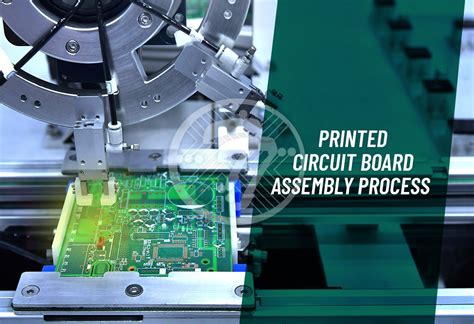
Implementing rigorous manufacturing protocols is critical for producing reliable PCBA control boards The transition from design to production demands precision in PCB assembly workflows, beginning with component placement accuracy and solder paste application Automated stencil printing ensures consistent deposition of solder paste, minimizing voids that could compromise electrical connections
Tip: Maintain a controlled environment (20–25°C, 40–60% humidity) during PCBA fabrication to prevent moisture absorption in sensitive components, which can lead to delamination or popcorning during reflow
Leveraging surface-mount technology (SMT) for high-density layouts optimizes space utilization while reducing parasitic inductance Post-reflow inspection via automated optical inspection (AOI) systems identifies defects like tombstoning or misaligned ICs early, preventing costly rework For mixed-technology boards requiring through-hole components, selective soldering systems offer precision without affecting adjacent SMT parts
Adherence to industry-proven cleaning protocols eliminates flux residues that might cause corrosion or short circuits Functional testing under simulated operational loads validates signal integrity and power distribution across the control board
Suggestion: Implement traceability systems to track batch-specific data, such as solder paste lot numbers or reflow profiles, streamlining root-cause analysis if field failures occur
Finally, collaboration between design and manufacturing teams ensures DFM (Design for Manufacturing) principles are prioritized, balancing performance requirements with assembly feasibility By integrating these practices, manufacturers achieve repeatable quality in PCBA production while scaling efficiently
Quality Validation Techniques in PCBA Production
Effective PCBA quality validation relies on a layered approach combining automated inspection, functional testing, and environmental stress screening Modern PCB assembly lines integrate automated optical inspection (AOI) systems to detect solder joint defects, component misalignment, and polarity errors at speeds exceeding 25,000 inspections per hour For hidden interconnects in multilayer boards, X-ray fluorescence (XRF) analysis verifies solder alloy composition, while boundary scan testing validates complex IC programming
Post-assembly functional testing employs in-circuit test (ICT) fixtures to measure electrical parameters against design specifications, ensuring PCBA control boards meet voltage tolerance and signal integrity requirements For mission-critical applications, environmental stress testing (ESS) subjects assemblies to thermal cycling (-40°C to +125°C) and vibration profiles, simulating 5+ years of operational wear in 72-hour accelerated tests
Advanced manufacturers now combine statistical process control (SPC) analytics with IoT-enabled traceability systems, correlating real-time production data with validation outcomes This data-driven approach reduces PCBA failure rates by 37% compared to conventional sampling methods, aligning with IPC-A-610 Class 3 standards for high-reliability electronics By embedding validation checkpoints throughout the PCB assembly workflow, engineers achieve first-pass yield improvements exceeding 92% while maintaining 01% field return rates
Thermal Management in PCBA Control Systems
Effective thermal management in PCBA design ensures long-term reliability by mitigating heat-related failures such as solder joint degradation or component drift Critical considerations begin with PCB assembly material selection—high-temperature substrates like polyimide or ceramic-filled laminates improve heat resistance, while copper thickness optimization balances conductivity and cost Component placement strategies, such as isolating heat-generating ICs from temperature-sensitive sensors, further enhance thermal performance
Advanced PCBA layouts integrate thermal vias and heat sinks to dissipate energy efficiently, particularly in high-power control systems Simulation tools like computational fluid dynamics (CFD) predict hotspots, enabling preemptive adjustments before prototyping For validation, engineers employ infrared thermography during PCB assembly testing to map thermal gradients and verify design compliance with industry standards like IPC-2221
Manufacturers also leverage active cooling solutions, including embedded fans or liquid cooling channels, for applications requiring precise temperature control However, these methods must align with DFM guidelines to avoid complicating assembly workflows By prioritizing thermal management early in the PCBA development cycle, teams reduce rework costs and ensure robust operation across environmental extremes
Implementing DFM Guidelines in PCBA Development
Effective implementation of Design for Manufacturing (DFM) principles is critical for optimizing PCBA control board development By establishing proactive design practices, engineers can mitigate production bottlenecks, reduce rework costs, and enhance the reliability of pcb assembly outcomes Key DFM considerations include component footprint standardization, which ensures compatibility with automated pick-and-place systems, and clearance optimization to prevent solder bridging during reflow processes
A systematic approach to DFM begins with collaborative reviews between design and manufacturing teams, focusing on material selection for thermal stability and mechanical durability For instance, specifying high-Tg substrates in areas prone to thermal stress improves pcba longevity in demanding environments Additionally, adhering to IPC-7351 land pattern standards minimizes placement inaccuracies while accommodating tolerance variations in surface-mount devices
Advanced pcb assembly workflows integrate DFM validation tools to simulate manufacturing scenarios, identifying potential issues like uneven copper distribution or inadequate via tenting This preemptive analysis reduces prototype iterations by 40-60%, accelerating time-to-market Manufacturers also prioritize panelization strategies to maximize substrate utilization and streamline depaneling processes without compromising board integrity
By embedding DFM protocols early in the pcba lifecycle, organizations achieve repeatable quality across high-volume production runs while maintaining compliance with industry-specific reliability benchmarks such as ISO 13845 or AEC-Q100 for automotive applications
Automated Assembly Innovations for PCBAs
Modern PCB assembly processes have undergone transformative changes through automation, significantly enhancing precision and scalability in PCBA manufacturing Robotic pick-and-place systems now achieve placement accuracies within ±25 microns, enabling error-free handling of miniature components such as 01005 packages and micro-BGAs These systems integrate machine vision technologies to verify component orientation and solder paste deposition in real time, reducing rework rates by up to 40% compared to manual methods
A key advancement lies in closed-loop feedback mechanisms that dynamically adjust process parameters during high-speed soldering For example, automated optical inspection (AOI) systems equipped with AI algorithms can detect solder bridging or tombstoning defects with 997% accuracy, directly feeding correction data to reflow ovens This synergy between inspection and process control ensures consistent PCBA quality while maintaining throughput speeds exceeding 25,000 components per hour
Modular assembly lines further optimize flexibility, allowing rapid changeovers between PCB assembly configurations without compromising cycle times Dual-lane conveyors and adaptive feeder systems support mixed-product manufacturing, critical for industries requiring small-batch prototypes alongside mass production By integrating these innovations, manufacturers achieve first-pass yield improvements of 15–20%, directly translating to reduced lead times and enhanced reliability in control board applications
Cost-Effective PCBA Manufacturing Processes
Achieving cost efficiency in PCBA production requires balancing quality with optimized workflows A critical starting point is material selection—choosing components that meet performance specifications without over-engineering By leveraging PCB assembly design for manufacturability (DFM) principles, engineers can minimize rework and reduce waste, such as avoiding overly complex layouts that increase fabrication time
Automation plays a pivotal role in lowering expenses High-speed pick-and-place machines and automated optical inspection (AOI) systems accelerate PCBA assembly while maintaining precision, reducing labor costs and human error Additionally, batch processing optimizes material usage, particularly for high-volume orders
Collaboration with suppliers to standardize component packages and negotiate bulk pricing further drives down costs Implementing just-in-time inventory management ensures parts arrive as needed, avoiding storage overhead For prototyping or low-volume runs, partnering with manufacturers offering flexible pricing models—such as panel-sharing programs—can yield significant savings
Finally, integrating testability early in the design phase prevents costly post-production fixes In-circuit testing (ICT) and functional validation during PCB assembly streamline quality checks, ensuring defects are caught before full-scale manufacturing By aligning these strategies, businesses can achieve reliable PCBA outcomes without compromising budgetary constraints
Conclusion
The development of PCBA control boards represents a strategic convergence of engineering precision and manufacturing excellence Successful implementations hinge on balancing PCB assembly best practices with rigorous design validation protocols, ensuring both functional integrity and production scalability As industries demand higher reliability in compact form factors, manufacturers must prioritize thermal optimization and automated assembly techniques that align with evolving industry benchmarks
Cost-effective production does not equate to compromised quality when employing DFM-driven approaches from the initial design phase By integrating PCBA validation processes that address both electrical performance and mechanical durability, engineers can mitigate risks in mission-critical applications The future of control board technology lies in adaptive manufacturing ecosystems that leverage data analytics for predictive maintenance and process refinement
Ultimately, the intersection of advanced component integration and PCB assembly innovations creates opportunities for developing next-generation electronics Organizations that maintain cross-disciplinary collaboration between design and manufacturing teams will continue leading in sectors requiring high-density, reliable control systems This holistic approach ensures PCBA solutions meet not only current technical specifications but also adapt to emerging technological demands
FAQs
What design factors most impact pcb assembly reliability?
Component placement, solder pad geometry, and material compatibility directly affect PCBA durability Implementing thermal relief patterns and adhering to IPC-2221 spacing standards minimizes stress during thermal cycling
How does automated optical inspection (AOI) enhance PCBA quality control?
AOI systems detect solder bridging, misaligned components, and missing parts with 992% accuracy, reducing post-assembly rework by 40-60% compared to manual checks
Why is impedance matching critical in high-frequency control board designs?
Mismatched traces cause signal reflection and data corruption, particularly in circuits operating above 100MHz Controlled dielectric materials and precision etching maintain impedance tolerances within ±10%
What DFM guidelines prevent manufacturing defects in pcb assembly?
Requiring 025mm annular rings for vias, avoiding acute-angle traces, and specifying solder mask expansion values between 50-75μm ensures compatibility with high-speed pick-and-place systems
How do conformal coatings extend PCBA operational lifespan?
Acrylic or silicone-based coatings provide moisture resistance (>500hrs salt spray protection) while allowing easier rework compared to epoxy alternatives
Optimize Your Next PCBA Project
For tailored design-for-manufacturing solutions and advanced pcb assembly capabilities, please click here to explore our certified production services