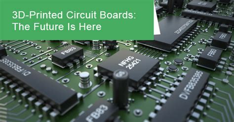
Pioneering 3D Printed PCB Manufacturers Shaping Electronics
Key Takeaways
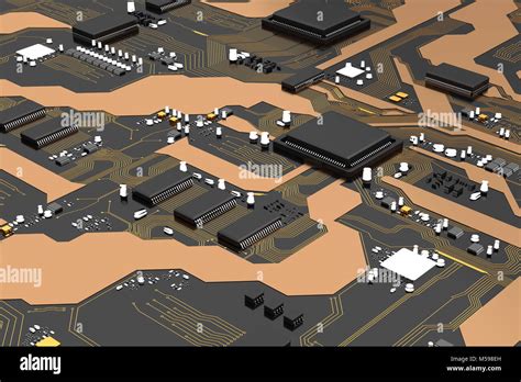
When exploring modern PCB manufacturing, you’ll find that 3D printed PCB manufacturing companies are redefining efficiency and sustainability. Innovations like conductive ink and *AME (https://www.andwinpcba.com) integrate multi-material printing systems, allowing you to produce functional circuits in hours rather than weeks. Meanwhile, firms like Nano Dimension prioritize eco-friendly practices, using recyclable materials to align with global sustainability goals.
For businesses considering a PCB manufacturing business, additive manufacturing offers scalability—whether for aerospace-grade components or educational kits. The ability to iterate designs rapidly reduces material waste, making it ideal for low-volume, high-mix production. As rapid prototyping becomes mainstream, PCB manufacturing companies leveraging 3D printing are positioned to dominate next-gen electronics markets. By adopting these technologies, you gain flexibility in design complexity while maintaining cost-efficiency—a critical advantage in fast-paced industries.
D Printed PCB Manufacturing Breakthroughs
Advancements in 3D printed PCB manufacturing now allow you to prototype complex circuits faster and with greater precision. Traditional PCB manufacturing companies often rely on subtractive methods, which generate significant waste and increase PCB manufacturing cost. In contrast, additive manufacturing techniques use conductive inks and AME (Additively Manufactured Electronics) technology to build circuits layer by layer, slashing material waste by up to 70%. This shift not only aligns with sustainability goals but also opens doors for smaller PCB manufacturing business ventures to enter the market without heavy upfront investments.
Tip: When evaluating your next project, consider how additive methods could reduce your PCB manufacturing cost while accelerating development cycles.
For instance, companies leveraging rapid prototyping can iterate designs in hours instead of weeks. The table below highlights key differences:
| Factor | Traditional PCB Manufacturing | 3D Printed PCB Manufacturing |
|---|---|---|
| Material Waste | High | Low |
| Production Time | 2–6 weeks | 1–3 days |
| Setup Costs | $10,000+ | <$5,000 |
| Design Flexibility | Limited | High |
This approach also supports eco-friendly solutions, as water-based conductive inks replace toxic etching chemicals. By integrating these innovations, businesses can address niche markets like aerospace or educational kits, where custom PCB manufacturing is critical but volume demands are lower.
Conductive Ink Innovations in Circuit Prototyping
When exploring modern PCB manufacturing, you’ll find that conductive inks are rewriting the rules of circuit prototyping. Unlike traditional etching methods, these advanced materials—often infused with silver nanoparticles or graphene—enable direct printing of conductive pathways onto flexible substrates. For PCB manufacturing companies, this innovation slashes PCB manufacturing cost by eliminating costly copper-clad laminates and reducing material waste. Imagine designing a prototype in hours instead of days: conductive ink systems let you iterate rapidly, testing ideas without waiting for external fabrication partners.
The shift isn’t just about speed. By integrating additive manufacturing techniques, businesses in the PCB manufacturing business can now produce multi-layered boards with embedded components, bypassing assembly steps. This approach also supports eco-friendly practices, as conductive inks often contain fewer toxic chemicals than conventional processes. Tools like aerosol jet printing even allow for micron-scale precision, critical for high-frequency or miniaturized devices.
For engineers and startups, these advancements mean lower barriers to entry. You no longer need massive capital to experiment with complex designs—desktop printers equipped with conductive inks bring prototyping in-house. As this technology matures, it’s reshaping how PCB manufacturing companies balance innovation with scalability, setting the stage for smarter, more adaptable electronics production.
AME Technology Reshaping Electronics Production
Additive Manufacturing Electronics (AME) is fundamentally altering how PCB manufacturing companies approach production. By layering conductive and insulating materials with precision, this method eliminates traditional subtractive processes, reducing material waste by up to 70% and slashing PCB manufacturing cost for complex designs. Imagine creating multilayer circuits in hours instead of weeks—AME enables rapid iteration, letting you test prototypes before committing to mass production.
Central to this shift are advancements like nanoparticle conductive inks, which allow finer traces and higher-density interconnects than conventional etching. These innovations aren’t just theoretical; they’re already empowering businesses to bypass costly tooling steps while maintaining performance standards. For startups or enterprises scaling IoT devices, AME’s flexibility supports both low-volume custom orders and high-throughput runs, redefining the economics of the PCB manufacturing business.
Critically, AME integrates seamlessly with digital workflows. Designers upload schematics directly to printers, minimizing human error and accelerating time-to-market. This digitally native approach also aligns with sustainability goals, as localized production cuts transportation emissions. Whether you’re optimizing existing lines or exploring additive methods, AME positions PCB manufacturing as a driver of agile, eco-conscious innovation—no longer a bottleneck but a strategic asset.
Eco-Friendly PCB Solutions With Additive Manufacturing
When evaluating PCB manufacturing options, you might find traditional methods generate significant chemical waste and energy consumption. Additive manufacturing, however, introduces resource-efficient alternatives by layering materials precisely, reducing excess use. Leading PCB manufacturing companies now integrate conductive inks and biodegradable substrates to minimize environmental impact. For instance, printing circuits layer-by-layer eliminates up to 70% of material waste compared to subtractive etching—a critical shift for lowering PCB manufacturing cost while supporting sustainability goals.
Adopting additive processes also allows businesses to align with circular economy principles. Water-based conductive inks replace hazardous solvents, and recyclable thermoplastics enable easier end-of-life processing. This approach not only streamlines PCB manufacturing business operations but also meets tightening regulations on electronic waste. By prioritizing closed-loop systems, manufacturers reduce reliance on rare metals and lower their carbon footprint without compromising circuit performance.
Transitioning to eco-friendly methods doesn’t mean sacrificing speed. Advanced additive systems maintain rapid prototyping capabilities, ensuring you can iterate designs quickly while adhering to greener practices. As industries demand both innovation and environmental responsibility, these solutions position additive manufacturing as a bridge between high-performance electronics and planetary stewardship.
Rapid Prototyping for Next-Gen Electronics Design
When designing cutting-edge electronics, PCB manufacturing timelines often dictate project feasibility. Traditional methods require weeks for iterative testing, but additive manufacturing slashes this to days—or even hours—by enabling direct digital-to-physical conversion. Leading PCB manufacturing companies now leverage conductive inks and multi-material deposition systems to print functional circuits in a single pass, bypassing photolithography and etching. This shift not only reduces PCB manufacturing cost by minimizing material waste but also empowers engineers to test complex geometries impractical with subtractive techniques.
For startups and R&D teams, rapid prototyping unlocks agility. Imagine adjusting trace layouts overnight or embedding components mid-print—a game-changer for IoT devices or wearables. The PCB manufacturing business is evolving beyond mass production; low-volume, high-mix orders thrive with on-demand printing. By integrating simulation software, you can validate designs virtually before printing, further compressing development cycles.
However, balancing speed with reliability remains critical. Advanced quality assurance protocols ensure prototypes meet industrial standards, even as layer resolutions approach 10μm. As aerospace and education sectors adopt these tools, the gap between concept and functional hardware narrows, redefining what’s possible in electronics innovation.
BotFactory’s Integrated PCB Printing Systems
When exploring advancements in PCB manufacturing, you’ll find companies like BotFactory redefining how circuits are designed and produced. Their integrated systems combine additive manufacturing with conductive ink innovations, enabling teams to prototype complex designs in hours rather than weeks. For PCB manufacturing companies aiming to reduce PCB manufacturing cost, BotFactory’s approach eliminates traditional etching processes, cutting material waste by up to 60% while maintaining precision.
What sets these systems apart is their seamless workflow—from CAD design to functional board—within a single platform. This integration is critical for startups or R&D teams in the PCB manufacturing business, where agility and iteration speed determine market competitiveness. By leveraging AME (Additively Manufactured Electronics) technology, users can print multilayer boards with embedded components, bypassing assembly steps that traditionally inflate timelines.
Moreover, BotFactory’s solutions address scalability challenges. Whether you’re testing a niche IoT sensor or refining aerospace-grade circuits, their printers adapt to low-volume runs without sacrificing quality—a game-changer for industries prioritizing customization. As sustainability gains traction, the reduced chemical usage and energy efficiency of these systems align with eco-conscious shifts in PCB manufacturing, proving that innovation doesn’t have to come at an environmental cost.
Nano Dimension’s Sustainable AME Advancements
When exploring PCB manufacturing companies committed to sustainability, you’ll find Nano Dimension’s advancements in additive manufacturing electronics (AME) redefine how circuits are produced. By leveraging proprietary conductive inks and precision deposition technologies, their systems eliminate traditional etching processes, reducing chemical waste and energy consumption. This approach not only lowers PCB manufacturing cost but also aligns with eco-conscious production goals—a critical advantage for businesses aiming to minimize environmental impact.
Their DragonFly IV system enables rapid prototyping of multi-layer boards, allowing you to test designs faster while maintaining high-resolution performance. For PCB manufacturing businesses, this means shorter lead times and the flexibility to iterate without costly tooling changes. Nano Dimension’s focus on closed-loop material systems further ensures minimal resource waste, making it a standout choice for industries prioritizing circular economy principles.
By integrating AME into your workflow, you gain access to scalable solutions that support both low-volume customization and high-volume demands. Whether optimizing PCB manufacturing for aerospace applications or educational prototypes, Nano Dimension’s innovations demonstrate how sustainability and efficiency can coexist in modern electronics production.
3D Printed Circuits for Aerospace and Education
When exploring advanced applications of PCB manufacturing, you’ll find 3D-printed circuits bridging critical gaps in aerospace innovation and educational accessibility. Aerospace demands lightweight, high-performance electronics capable of withstanding extreme conditions—a challenge traditional PCB manufacturing companies often struggle to address cost-effectively. By leveraging additive techniques, engineers create complex, multi-layered designs with design freedom unmatched by conventional methods, reducing PCB manufacturing cost while enhancing durability in satellites, drones, and avionics systems.
In education, 3D printing democratizes access to circuit prototyping. Universities and STEM programs now integrate desktop PCB printers, allowing students to iterate designs without relying on external PCB manufacturing business partners. This hands-on approach accelerates learning, as learners troubleshoot real-world constraints like conductive ink adhesion or layer alignment. For instance, aerospace-grade materials tested in labs double as teaching tools, showcasing how rapid prototyping reshapes both industries.
The synergy between aerospace rigor and educational experimentation highlights how additive manufacturing isn’t just a niche tool—it’s redefining scalability across PCB manufacturing workflows. Whether optimizing satellite components or empowering future engineers, 3D-printed circuits prove that on-demand production and sustainability can coexist in high-stakes and classroom environments alike.
Conclusion
As additive manufacturing reshapes PCB manufacturing, you’re witnessing a fundamental shift in how electronics ecosystems operate. The integration of 3D printing technologies enables PCB manufacturing companies to bypass traditional limitations, offering unprecedented flexibility in design iteration and material usage. By slashing PCB manufacturing cost through reduced material waste and streamlined workflows, these innovators make rapid prototyping accessible even for small-scale projects.
For businesses evaluating their PCB manufacturing business strategies, adopting additive methods isn’t just about staying competitive—it’s about aligning with sustainable practices that minimize environmental footprints. Advanced conductive inks and AME-driven processes further ensure precision while maintaining scalability, critical for industries ranging from aerospace to educational prototyping.
This evolution isn’t merely technical—it’s redefining economic and ecological benchmarks across the sector. As these technologies mature, they’ll continue lowering barriers to entry, empowering more creators to turn concepts into functional circuits without compromising on performance or sustainability. The future of electronics lies in embracing these transformative tools today.
FAQs
How does 3D printing reduce pcb manufacturing cost compared to traditional methods?
By eliminating tooling and minimizing material waste, additive manufacturing slashes upfront investments. PCB manufacturing companies leveraging conductive inks and AME tech avoid costly etching processes, making short-run production economically viable for startups and educators.
What advantages do pcb manufacturing businesses gain with rapid prototyping?
Iterating designs in hours—not weeks—accelerates product development cycles. Technologies like BotFactory’s integrated systems enable real-time adjustments, reducing errors and ensuring faster time-to-market for IoT or aerospace applications.
Are 3D-printed circuits reliable for industrial use?
Advanced materials like Nano Dimension’s conductive inks meet stringent thermal and electrical standards. While not yet universal, they’re increasingly adopted for low-volume, high-mix production in sectors valuing customization over mass scale.
How sustainable is additive manufacturing for pcb manufacturing?
Eco-friendly practices, such as solvent-free inks and energy-efficient printers, reduce carbon footprints. Companies prioritizing circular workflows now recycle 60–70% of unused materials, aligning with global sustainability mandates.
Where can you explore custom 3D-printed PCB solutions?
Discover Tailored PCB Manufacturing Options
For prototyping or specialized projects, click here to connect with experts optimizing additive techniques for your industry’s needs.


