Post-Layout PCB Checklist: Essential Verification Steps Before Manufacturing
After completing the PCB (Printed Circuit Board) layout, a thorough review is crucial to ensure functionality, reliability, and manufacturability. Skipping this step can lead to costly errors, delays, or even complete board failures. This article outlines a comprehensive checklist of critical verification steps before finalizing your PCB design for production.
1. Design Rule Check (DRC)
The first step is running a Design Rule Check (DRC) to ensure the layout adheres to predefined constraints. Key aspects include:
- Trace Width and Spacing: Verify that trace widths meet current-carrying requirements and spacing complies with voltage isolation needs.
- Clearance Rules: Ensure adequate clearance between traces, pads, and vias to prevent short circuits.
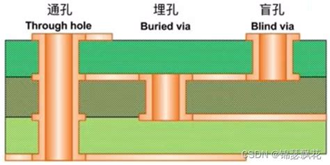
- Via Sizing: Confirm via diameters and annular rings meet manufacturing capabilities.
- Copper-to-Edge Clearance: Check that copper traces and planes are sufficiently spaced from the board edge to avoid shorts during fabrication.
2. Electrical Rule Check (ERC)
An Electrical Rule Check (ERC) ensures logical and electrical correctness:
- Unconnected Nets: Detect floating pins or missing connections.
- Short Circuits: Identify accidental overlaps or unintended connections.
- Power and Ground Integrity: Verify that all power and ground nets are correctly connected.
- Pin Compatibility: Ensure component pins match schematic symbols (e.g., no swapped pins).
3. Signal Integrity (SI) Analysis
High-speed designs require Signal Integrity (SI) checks:
- Impedance Matching: Verify controlled impedance traces (e.g., 50Ω for RF, 90Ω for USB differential pairs).
- Crosstalk Analysis: Ensure minimal interference between adjacent traces.
- Reflections and Ringing: Check for excessive overshoot/undershoot due to impedance mismatches.
- Timing Delays: Confirm signal propagation meets timing requirements (critical for clocks and high-speed interfaces like DDR, PCIe).
4. Power Integrity (PI) Verification
A stable power distribution network (PDN) is essential:
- Voltage Drop Analysis: Ensure minimal IR drop across power rails.
- Decoupling Capacitor Placement: Verify proper placement near IC power pins.
- Power Plane Splits: Check for adequate current return paths and avoid splits under high-speed signals.
- Ground Loops: Prevent ground inconsistencies that could introduce noise.
5. Thermal Analysis
Overheating can degrade performance or damage components:
- Current Density in Traces: Ensure traces can handle expected current without excessive heating.
- Thermal Relief Pads: Verify proper thermal connections for soldering.
- Component Placement: Check heat-generating components (e.g., regulators, processors) for adequate spacing and cooling.
6. Manufacturing (DFM) and Assembly (DFA) Checks
Design for Manufacturability (DFM) and Design for Assembly (DFA) reduce production issues:
- Minimum Trace/Space: Confirm compliance with the PCB fab’s capabilities.
- Solder Mask and Silkscreen: Ensure no overlaps, legible text, and proper solder mask coverage.
- Component Footprints: Verify pad sizes, spacing, and orientation match datasheets.
- Pick-and-Place Compatibility: Check component spacing for automated assembly.
- Test Point Accessibility: Include test points for debugging and validation.
7. Mechanical and 3D Fit Check
Physical constraints must be validated:
- Board Dimensions: Match the enclosure or mechanical drawings.
- Component Heights: Ensure no collisions with enclosures or other boards.
- Mounting Holes: Verify correct placement and clearance for screws/standoffs.
- Connector Alignment: Check mating connectors align properly.
8. EMI/EMC Consideration
Prevent electromagnetic interference (EMI) and ensure compliance:
- Grounding Strategy: Confirm a solid ground plane with minimal splits.
- Shielding: Add shielding cans or grounded copper pours for sensitive circuits.
- High-Speed Signal Routing: Avoid long parallel runs that act as antennas.
- Filtering Components: Place ferrite beads and capacitors near noise sources.

9. Documentation Review
Accurate documentation prevents assembly errors:
- Bill of Materials (BOM): Verify part numbers, quantities, and substitutions.
- Assembly Drawings: Include reference designators, polarity markings, and orientation notes.
- Gerber Files: Cross-check layers (copper, solder mask, silkscreen, drill files).
- Fabrication Notes: Specify material, finish (ENIG, HASL), impedance control, and testing requirements.
10. Final Visual Inspection
A manual review catches subtle errors:
- Unrouted Nets: Look for missing connections (highlighted in CAD tools).
- Stray Copper: Remove isolated copper islands that could cause shorts.
- Silkscreen Errors: Ensure readable and correctly placed labels.
- Via Tenting: Confirm whether vias should be covered (tented) or open.
Conclusion
A systematic post-layout PCB verification process minimizes risks and ensures a successful manufacturing outcome. By following this checklist—covering DRC/ERC, signal/power integrity, thermal, DFM/DFA, mechanical, EMI, and documentation—you can avoid common pitfalls and deliver a robust, reliable PCB design. Always collaborate with your fabrication and assembly partners to align with their specific requirements before finalizing the design.