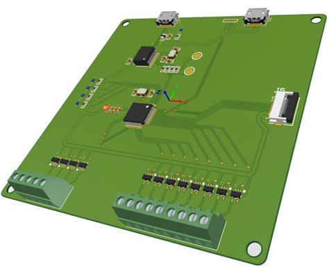
Power integrity simulation makes the circuit board more perfect
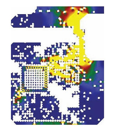
Digital chips require large currents, which may cause problems in supplying DC power (Reference 2). FPGAs and other digital chips require a variety of power supply voltages, so the power plane must be split to provide multiple voltage rails. Digital chips also have hundreds of pins, requiring hundreds of vias, which will cover a large copper area of the power and ground layers. It is necessary to ensure that the current density remains below a reasonable value on the copper selected for these layers (Figure 5).
High DC currents can also cause thermal problems. The temperature coefficient of copper is 0.4%/°C, which means that for every 25°C increase in temperature, the resistance increases by 10%. This increase in resistance occurs under heavy loads, when reliability is critical. The increase in resistance also increases the temperature, reducing the life of components on the circuit board.
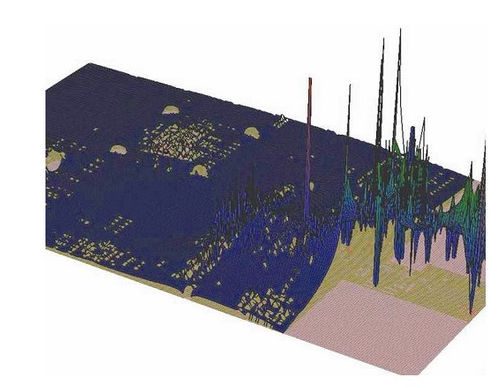
Once there is sufficient copper to provide DC loads, pay attention to the AC design of the power layer (Figure 6).
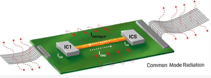
Power integrity simulation checks where the return current flows through the power plane. During operation, a digital chip sees different current levels that vary in nanoseconds. The power system must have low enough AC impedance to change with the current (expressed as di/dt, current derivative/time derivative) so that the supply voltage at the chip pins does not change significantly. Because di/dt also radiates electromagnetic energy, these excursions can cause EMI problems. Therefore, signal integrity, power integrity, and EMI compliance are all interrelated. Without simulation, your design may have crosstalk between vias and other seemingly inexplicable problems.
Software Selection
The actual geometry of a power network is so important to its performance that most software vendors use field solver technology in their power integrity tools (Reference 3).
These tools should give you a quick answer and accurate results. RF-IC and system designers typically use full-wave field solvers to solve Maxwell’s equations in 3D. However, 3D field solvers take a long time to produce results, especially when used on relatively large physical items such as PCB boards. As a result, power-integrity vendors have designed hybrid solver technology into their power-integrity tools. When solving traces, these tools use a 2D solver that uses fast techniques from transmission-line theory. When simulating planes, the tools can use 2D or 2.5D finite-element techniques. In some cases, the software can model vias using a lumped-element model of capacitance and inductance. For more accurate results, the tool can use a full-wave 3D solver for vias.
In addition, a full-wave solver can be used to simulate the effects of 3D structures, such as connector pins and other mechanical devices in the power path. Software vendors have also built thermal analysis capabilities into their tools. You can use it standalone or export the thermal information to a dedicated thermal analysis tool, such as Mentor Graphics’ FloTherm, a 3D simulation environment for CFD (computational fluid dynamics). Mentor’s HyperLynx simulation tool can do its own thermal analysis and export the results to FloTherm, which can model the thermal performance of an entire system or a chassis.
Agilent has redeveloped its ADS (Advanced Design System) Momentum product to provide simulation results for power and ground planes with a high number of vias. It can also be used for designs with a small number of traces on the power plane. The fastest simulation method for multilayer structures is the MOM (Method of Moments), which solves the full 3D field, including all the terms in Maxwell’s equations. This full-wave approach takes into account the high-frequency effects of Faraday’s law and the substitution current terms that Maxwell adds to the Ampère equations (Reference 4). Simulating large layers with MOM is very time-consuming, so Agilent has developed algorithms that reduce the time required to obtain accurate results. Colin Warwick, owner of high-speed digital products at Agilent, said the tool uses a tree/co-tree approach that works all the way down to DC.
It is also possible to use lumped parameter analysis for planar components.
NEC’s PIStreamn software models planes as matrices of lumped parameters, making them suitable for analysis using Spice engines and other lumped parameter techniques. For a plane, the software generates an equivalent of an RLGC (resistance/inductance/conductance/capacitance) using PEEC (partial element equivalent circuit) technology. The software also creates lumped parameter models for vias and the cavity formed between the power plane and the ground plane (Figure 7). The software also models the decoupling capacitors using a series RLC (resistance/inductance/capacitance) model that takes into account the parasitic resistance and capacitance of the capacitors as well as the parasitic resistance and inductance of the fan-out traces and vias. You can quickly complete the analysis of a single board pair by setting up a simulation run. When you change the settings, the software will do a multi-layer analysis that takes into account all related boards.
In addition to simulating the physical structure of the finished board, software tools such as HyperLynx can also do early floor planning of board layers and decoupling structures. Then you can quickly run an analysis to get some ideas about transfer impedance and other variables. Giga Hertz Technology has developed a faster Spice engine and integrated it into NEC’s PDN (power distribution network) Expert. These floorplanning tools allow you to manually outline the PCB and layers to optimize capacitance early in the design process. This gives you an idea of the board shape, size, stackup, and number of capacitors.
Some PC-based power-integrity software vendors, such as Mentor Graphics and Cadence, have integrated their tools into the design flow. While this doesn’t eliminate the worry of having one vendor provide all the tools, power-integrity simulation uses a physical representation of the PCB, a geometric model. Ansys and Sigrity both accept input from tools from Cadence’s Allegro, Mentor Graphics’ PADS, and companies such as Zuken and Altium. Agilent’s power-integrity tools are derived from its expertise in RF design. In addition to working with ADS design tools, the company’s EMPro software can also input PCB data from Cadence’s Allegro. Customers often use NEC’s PIStream with Zuken’s PCB tools, but the software can also accept input from Cadence’s Allegro and other PCB software.
Although some engineers prefer integrated tools in their own board flow, there are some advantages to getting tools from simulation specialists like Ansys. For example, the company’s SI (signal integrity) Wave tool is similar to Mentro Graphics’ HyperLynx, while the PIAdvisor tool can help you drill down into power integrity issues. The tool has a 3D solver for via simulation. Alternatively, you can use Ansys’ HFSS (High Frequency Simulator System) tool to do full 3D simulation of physical problems, such as connectors and other 3D geometries. Some customers feed the output of Ansys power integrity tools and signal integrity tools into the same HFSS tool they use to model the chassis. This allows them to evaluate the EMI of their products. CST (Computer Simulation Technology) EM Studio software accepts Gerber PCB file inputs and can calculate 3D IR (current/resistance) drops.
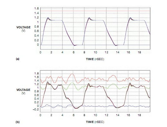
The software you choose must have the capabilities you need. Many companies want you to solve signal integrity and power integrity issues separately, assuming that once you have sufficiently reduced the power supply impedance, you will focus on signal integrity. The problem with this approach is that power supply noise interacts with signal noise. To address this problem, Sigrity allows you to simulate the effects of power noise on signal integrity (Figure 8). CST’s Microwave Studio can also analyze noise propagating from closely spaced power planes.
High Price Issue
The price of power-integrity software often makes inexperienced engineers gasp. A simple DC simulator can cost $15,000, while a complete system that includes power integrity, signal integrity, and thermal solvers can cost $75,000. That number may seem high for software, but the cost of a power-integrity failure should be considered. A complex board remake can cost $5,000 or $10,000 in manufacturing and engineering, and $1 million in delays to market. Another consideration is the system’s BOM (bill of materials) cost. If power-integrity software can save 50 cents on capacitors, it can pay for itself in a few months for a high-volume product.
Ansys’ Patel found that the three engineers doing power integrity, signal integrity, and EMI analysis were isolated from each other. Today, while one engineer may still do EMI analysis, that person will work with someone who does power-integrity and signal-integrity analysis first, and they often share the same software. Sigrity’s Brim points out that IBIS
(Input/Output Buffer Specification) 5.0 has power-ground
and signal data, allowing simulation software to relate the noise on the 5.0 model’s power pins to the noise leaking through the output, similar to the PSRR specification in analog devices. All of these features combine to give you a well-designed, reliable product (Figure 9).
If you understand and know how to use these expensive tools, you’ll be doubly effective as an engineer. For engineers who prefer CAD (computer-aided design) software, these tools are not difficult to learn. Mentor Graphics offers free courses on HyperLynx at many of its sales locations. If you have experience with other types of simulators, learning power-integrity tools is pretty straightforward. What needs to be learned and understood are the concepts and terminology of the frequency domain, as RF designers do. If you add this knowledge to your existing time-domain experience, you can take on the most stringent design challenges and come out a winner.