Power module PCB design
The power circuit is an important part of an electronic product. The quality of the power circuit design directly affects the performance of the product. The power circuits of our electronic products mainly include linear power supplies and high-frequency switching power supplies. Theoretically, the linear power supply is how much current the user needs, and the input end must provide how much current; the switching power supply is how much power the user needs, and the input end provides how much power.
Linear power supply
Linear power supply power devices work in a linear state, such as our commonly used voltage regulator chips LM7805, LM317, SPX1117, etc. The following figure is the schematic diagram of the LM7805 voltage regulator circuit.
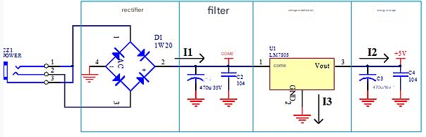
Figure 1 Linear power supply schematic diagram
As can be seen from the figure, the linear power supply consists of functional components such as rectification, filtering, voltage regulation, and energy storage. At the same time, the generally used linear power supply is a series voltage regulator, and the output current is equal to the input current, I1=I2+I3, I3 is the reference end, and the current is very small, so I1≈I3. Why do we talk about current? Because when designing PCB, the width of each line is not set randomly, but is determined according to the current size between the component nodes in the schematic diagram (please refer to the “PCB Design Copper Platinum Thickness, Line Width and Current Relationship Table”). The current size and current flow direction must be clear to make the board just right.
When designing PCB, the layout of components should be compact, all connections should be as short as possible, and the components and routing should be arranged according to the functional relationship of the components in the schematic diagram. In this power supply diagram, rectification first, then filtering, voltage stabilization after filtering, energy storage capacitor after voltage stabilization, and power supply to the subsequent circuit after flowing through the capacitor.
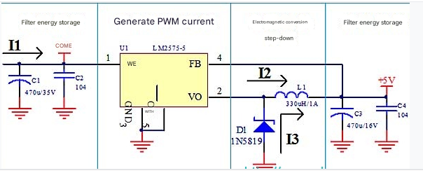
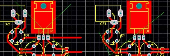
Figure 2 is the PCB diagram of the above schematic diagram, and the two diagrams are similar.
The left and right diagrams are slightly different in routing. The power supply in the left diagram directly reaches the input pin of the voltage stabilizing chip after rectification, and then the voltage stabilizing capacitor. The filtering effect of the capacitor here is much worse, and there are also problems with the output. The right diagram is a better diagram. We must not only consider the flow direction of the positive power supply, but also the ground return problem. Generally speaking, the positive power line and the ground return line should be as close to each other as possible.
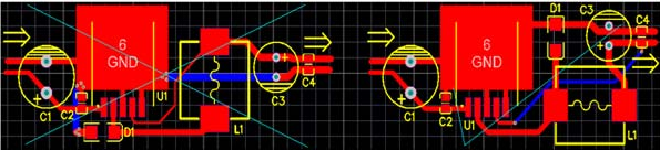
Figure 4 Linear power supply PCB diagram
When designing a linear power supply PCB, we should also pay attention to the heat dissipation of the power regulator chip of the linear power supply, and how the heat comes. If the front-end voltage of the regulator chip is 10V, the output end is 5V, and the output current is 500mA, then there is a 5V voltage drop on the regulator chip, and the heat generated is 2.5W; if the input voltage is 15V, the voltage drop is 10V, and the heat generated is 5W. Therefore, we need to leave enough heat dissipation space or a reasonable heat sink according to the heat dissipation power when laying out the board. Linear power supplies are generally used in occasions with relatively small voltage differences and relatively small currents. Otherwise, please use a switching power supply circuit instead.
High-frequency switching power supply
The switching power supply uses a circuit to control the switch tube to conduct high-speed conduction and cutoff, generate a PWM waveform, and adjust the voltage by electromagnetic conversion through an inductor and a freewheeling diode. The switching power supply has high power, high efficiency and low heat generation. The circuits we generally use are: LM2575, MC34063, SP6659, etc. In theory, the power at both ends of the switching power supply circuit is equal, the voltage is inversely proportional, and the current is inversely proportional.
Figure 3 Schematic diagram of the LM2575 switching power supply circuit
When designing the switching power supply PCB, you need to pay attention to: the introduction point of the feedback line and who the freewheeling diode is for. As can be seen from Figure 3, when U1 is turned on, the current I2 enters the inductor L1. The characteristic of the inductor is that the current cannot be generated suddenly or disappear suddenly when it flows through the inductor. The change of the current in the inductor has a time process. When the pulse current I2 flows through the inductor, part of the electric energy is converted into magnetic energy, and the current gradually increases. At a certain time, the control circuit U1 turns off I2. Due to the characteristics of the inductor, the current cannot disappear suddenly. At this time, the diode works and takes over the current I2, so it is called a freewheeling diode. It can be seen that the freewheeling diode is used for the inductor. The freewheeling current I3 starts from the negative end of C3 and flows into the positive end of C3 after passing through D1 and L1. This is equivalent to a pump, which uses the energy of the inductor to increase the voltage of the capacitor C3. There is also the problem of the introduction point of the feedback line of the voltage detection. It should be fed back to the place after filtering, otherwise it will make the output voltage ripple larger. These two points are often ignored by many of our PCB designers. They think that the same network is not the same when connected there. In fact, the performance is greatly affected by different connection places. Figure 4 is the PCB diagram of the LM2575 switching power supply. Let’s see where the wrong picture is wrong.
Figure 4 LM2575 switching power supply PCB diagram
Why do we need to explain the principle of the schematic diagram in detail? Because the schematic diagram contains a lot of information for drawing PCB, such as the access point of the component pins, the current size of the node network, etc. If you can see the schematic diagram clearly, PCB design will not be a problem. The LM7805 and LM2575 circuits represent the typical layout circuits of linear power supplies and switching power supplies respectively. When making PCBs, you can directly follow the layout and wiring of these two PCB diagrams. It’s just that the products are different, and the circuit boards are also different. Adjust according to the actual situation.
All changes are the same, so the principles and layout methods of power supply circuits are the same, and every electronic product cannot be separated from the power supply and its circuit. Therefore, after learning these two circuits, the others will also be clear in mind.


