Practical Design Tips for PCB Silk Screen Polarity Marking
In the field of PCB (printed circuit board) design, silk screen, as a key element on the surface of the circuit board, plays an important role. It provides engineers, production personnel and subsequent maintenance personnel with important information such as component number, location, installation direction, etc., and is the core element to ensure the readability and convenience of the circuit board.
A well-designed PCB silk screen marking can significantly improve work efficiency, reduce the risk of welding errors, and provide strong support for the production, testing, and maintenance of circuit boards. However, in the actual design process, there are often some problems with silk screen polarity marking, which requires our in-depth discussion and improvement.
1.Common problems with PCB silk screen polarity marking
In the practice of providing DFA (design for assembly) review services to many customers, we found that engineers have different habits of silk screen polarity marking. Some engineers use intuitive ** “+/-” symbols to mark positive and negative poles**, and some engineers use the triangle symbol of the diode to indicate the positive and negative directions. However, there are still many marking symbols with potential defects, which are easy to cause misunderstandings and bring troubles to the use and maintenance of circuit boards.
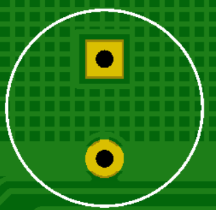
(1)Use dots to mark polarity
It is common to use dots to mark one side of the pad as a polarity symbol, but the problem is that different designers have different definitions of the polarity represented by dots. For non-circuit board designers, this marking method is difficult to accurately determine the positive and negative poles, which is very easy to cause misunderstandings, and thus affect the correct installation and maintenance of the circuit board.

(2)Use long and short silk screen lines on both sides to mark polarity
Similar to dot marking, this marking method also makes it difficult for users to determine whether the pad on the long line is positive or negative. In addition, in the actual drawing process, there may be only a slight difference in length between the silk screen lines on both sides, which undoubtedly further increases the difficulty for users to judge polarity and weakens the function of silk screen marking.
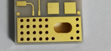
(3)Lack of silk screen marking
For plug-in components with polarity, some designers only change one of the via pads to a square pad to indicate polarity. However, the use of square pads to indicate PIN1 is different from the polarity requirements. These polarity pins do not clearly specify in the specification that PIN1 is positive or negative. Unless the device screen has an obvious asymmetric outline to assist in judgment, it is difficult to accurately determine the polarity direction for use, which brings great inconvenience to circuit board welding or maintenance.
2.Design suggestions for screen printing polarity marking
In order to effectively improve the identifiability and convenience of the circuit board and enhance the intuitiveness and accuracy of the screen printing polarity marking, we recommend the following design methods.
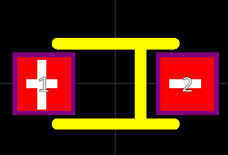
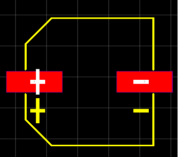
(1)”+/-” mark polarity or “K” mark negative pole
The “+/-” symbol is a well-known way to indicate positive and negative poles. Marking it clearly on the circuit board allows users to quickly and accurately identify the corresponding positions of positive and negative poles. This marking method is concise and clear, in line with the public’s cognitive habits, effectively avoiding misunderstandings caused by vague markings, and providing strong guarantees for the installation, testing and maintenance of circuit boards.
(2)Use a horizontal line on one side to mark polarity
When the actual component has a horizontal line for polarity marking, use a horizontal line to mark the polarity on the PCB accordingly, so that users can intuitively determine the positive and negative poles. This design method echoes the physical characteristics of components, enhances the recognition and credibility of silk screen marking, and helps improve the overall quality and reliability of circuit boards.
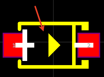
(3)Secondary tube triangle symbol marking
The conduction symbol of the diode is an intuitive polarity representation method. By using the diode triangle symbol to mark the polarity, users can easily determine the positive and negative poles according to the conduction direction. This marking method not only meets the professional specifications of the electronics industry, but also provides clear and accurate guidance for engineers and production personnel to ensure the correct installation and welding of circuit boards.
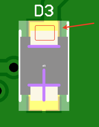
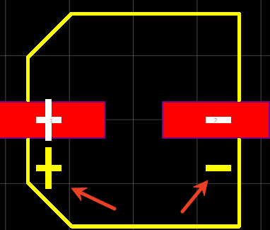
(4)Draw silk screen markings according to the physical frame
For non-completely symmetrical polarity plug-ins, adding the physical silk screen frame is an effective auxiliary judgment method. In this way, users can accurately understand the installation direction of components and determine the polarity according to the shape and direction of the silk screen frame. This not only improves the efficiency of polarity judgment, but also enhances the standardization and professionalism of circuit board design.
In summary, the use of a more intuitive and clear silk screen marking polarity design is of great significance for simplifying the PCB manufacturing and testing process and improving the overall quality of PCBs. Therefore, we hope that the above tips can provide useful reference and reference for your circuit board design.