Practical PCB panelization strategy, is your panelization reasonable?
Earlier we mentioned that PCB panelization is a crucial link, which not only affects the production efficiency of the product, but also directly affects the quality and cost of the product. Reasonable panelization can optimize the production process, reduce waste and increase production capacity.
However, in actual operation, due to the influence of various factors, many engineers have many problems with PCB panelization. This article will take you to explore the rationality and importance of PCB panelization, and help you to deeply understand how to optimize the panelization design, improve production efficiency and reduce costs. Let’s discuss together, is your panelization reasonable?
01 Basic requirements for panelization
When is panelization needed?
When one side of the length or width of the PCB single board is less than 50mm, it is recommended to design the panelization to improve production efficiency. Because when the designed panel size is smaller than the machine’s production size, the machine cannot produce it. The maximum size that Huaqiu can panelize is the maximum size: single and double-sided boards ≤6050cm, multi-layer boards ≤5040cm. Generally speaking, the efficiency of patching is guaranteed only when the panel size is controlled within this range.
Plate size
Stamp hole connection size (applicable to special-shaped plates): Plate size is greater than 50*50mm (to improve efficiency, it is recommended to make it as large as possible); special attention should be paid to the fact that the position of the stamp hole plate connection will be uneven in the shape of gears after being broken apart. V-cut size (applicable to square-shaped plates): Due to the requirements of V-cutting machine equipment, the length and width of the plate after the plate is at least 60mm, and the maximum size after the plate is 480mm;
Special attention should be paid to the fact that V-cutting only goes in a straight line, and double-sided V-cutting is the default, and single-sided V-cutting is not performed. The edges of the copper surface, wire/pad, etc. need to be more than 0.4MM away from the center line of the V-cut to avoid copper damage during V-cutting (in addition, the mounting hole should be as far away from the V-cut line as possible to avoid holes when breaking the plate).
Sheet utilization rate: the ratio of the shipping area to the large material area. The conventional ratio should be more than 85%, and low utilization will increase production costs. The recommended plate size is about 150*200mm. Huaqiu DFM has a utilization calculation function, which will automatically calculate the utilization rate of the panel cutting after the panel is assembled.

Technology edge requirements
The width of the technology edge is usually 5mm (minimum 3mm), with 4 positioning holes of 2mm diameter (no copper holes) added on it, and 4 asymmetrically distributed light spots: diameter 1mm (solder mask opening 2mm);
When the components on the PCB are less than 5mm away from the board edge and need to pass through the SMT guide rail, in order to facilitate assembly, a 5mm double-sided technology edge is usually added to the guide rail for production. For the wave soldering process, the component should be greater than 5mm away from the board edge.
Consistent panel direction
For boards with relatively regular shapes, the orientation of the single board in the panel should be kept consistent as much as possible to facilitate placement machines or manual operations;
02 Panel connection method
CNC+V-CUT panel
CNC plus V-cut panel is suitable for panels with devices on the edge of the panel, and cannot be panelized without spacing. The panel is assembled in the form of adding technology edges, with V-CUT treatment at both ends and a gong in the middle to facilitate welding of components. Otherwise, the devices on the edge of the board will interfere with each other and cannot be assembled and welded.
Stamp hole bridge assembly
Stamp hole is a bridge connection method for assembly. Stamp hole bridge connection can solve problems that V-CUT bridge connection cannot solve, such as round boards, irregular boards, etc. If V-CUT is not possible, stamp hole connection assembly can only be adopted.
V-CUT bridge assembly
V-CUT bridge assembly is suitable for regular boards. Since the V-CUT knife cannot turn, the V-CUT position must be a straight line. Note that components cannot be V-CUT when they are close to the edge of the board, otherwise it will affect the assembly and welding.
No process edge assembly
In order to save the utilization rate of the board material, no process edge assembly can be used. To ensure the convenience of production and assembly, there must be positioning holes and mark points in the board. And the mounting position must be greater than 5mm from the edge of the board, otherwise a jig will be required during assembly and welding, which will affect the cost.

03 Methods and skills of panelization
Interference of panelization components
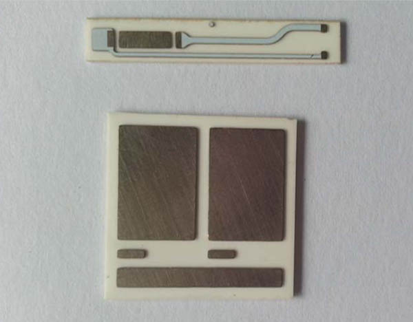
Peripheral connectors, including USB, TYPE-C, HDMI socket, TF card socket, SIM card socket, micro USB, headphone socket, RF connector, fiber cage, DC socket, MINI USB, audio and video socket, etc., need to be handled with caution. Especially when these devices exceed the edge of the board, appropriate spacing must be reserved for panelization to prevent interference with devices on other boards and inability to assemble components. See the figure below;
Adding sub-boards and stamp holes
When processing irregular-shaped board panelization, due to the lack of process edge connection, the board is easy to break, or the tin is overflowed and the board is deformed during wave soldering. To solve this problem, a sub-board can be added to the milling area, and then the PCB and the sub-board can be connected through the stamp hole. This can effectively prevent the PCB board from breaking or the wave soldering from overflowing and the board from deforming. See the figure below;
Half-hole must leave spacing
When processing half-hole board panelization, appropriate spacing must be reserved. This is because when drilling, if there is no spacing, the board next to it may be damaged. In addition, the use of no-spacing paneling for V-CUT molding will also damage the half hole, and may even tear the copper skin in the half hole. Therefore, in order to ensure the integrity and reliability of the half-hole board, the paneling must be performed in accordance with the appropriate spacing requirements. See the figure below;
V-CUT feed edge is not flush
When processing a board with uneven outer lines, the uneven side needs to leave a spacing paneling, and V-CUT processing cannot be performed. If there is no spacing paneling, the uneven side cannot be V-CUT; if the uneven side is paneled outward, the guide rail cannot be stuck, which will cause V-CUT deviation. To ensure processing quality and accuracy, the appropriate spacing and paneling direction must be followed. See the figure below;
04 Summary
This article explores the rationality and importance of PCB paneling, and introduces methods and techniques for optimizing paneling design. By deeply understanding the basic requirements, connection methods and methods and techniques of paneling, everyone can better master how to optimize paneling design, improve production efficiency and reduce costs. Due to the length of the article, we will stop here in this issue. In the next issue, we will share some practical cases of unreasonable panelization to help you understand the unreasonable scenarios of panelization. Finally, we recommend that you can use the panelization function of Huaqiu DFM, which can help you solve the unnecessary hidden dangers of panelization in production.