Precautions for copper wiring of PCB printed circuit boards of switching power supplies
1.Introduction
This article reference address:
Switching power supply is a voltage conversion circuit, the main working content is boost and buck, widely used in modern products. Because the switching transistor always works in the “on” and “off” states, it is called a switching power supply.
Switching power supply is essentially an oscillation circuit.
This way of converting electrical energy is not only used in power supply circuits, but also in other circuit applications, such as backlight circuits of LCD monitors, fluorescent lamps, etc. Compared with transformers, switching power supplies have the advantages of high efficiency, good stability, and small size. The disadvantage is that the power is relatively small, and it will generate high-frequency interference to the circuit. The transformer feedback oscillation circuit, which can generate regular pulse current or voltage, is called an oscillation circuit. The transformer feedback oscillation circuit is a circuit that can meet this condition.
Switching power supplies are divided into two forms, isolated and non-isolated. Here we mainly talk about the topological form of isolated switching power supplies. In the following text, unless otherwise specified, all refer to isolated power supplies.
Isolated power supplies can be divided into two categories according to different structural forms: forward and flyback.
Flyback refers to the working state in which the secondary side is cut off when the primary side of the transformer is turned on, and the transformer stores energy. When the primary side is cut off, the secondary side is turned on, and the energy is released to the load. Generally, conventional flyback power supplies have more single tubes, and double tubes are uncommon. Forward refers to the situation in which the primary side of the transformer is turned on and the secondary side senses the corresponding voltage and outputs it to the load, and the energy is directly transmitted through the transformer. According to the specifications, it can be divided into conventional forward, including single-tube forward and double-tube forward. Half-bridge and bridge circuits are both forward circuits.
Forward and flyback circuits each have their own characteristics. In the process of designing circuits, they can be used flexibly to achieve the best cost-effectiveness. Generally, flyback can be selected in low-power occasions. For slightly larger power supplies, a single-tube forward circuit can be used.
For medium power supplies, a double-tube forward circuit or a half-bridge circuit can be used. For low voltage, a push-pull circuit is used, which is the same as the working state of a half-bridge. For high power output, a bridge circuit is generally used, and a push-pull circuit can also be used for low voltage.
Flyback power supplies are widely used in small and medium power supplies because of their simple structure and the elimination of an inductor that is about the same size as the transformer. In some introductions, it is said that the power of a flyback power supply can only reach tens of watts, and there is no advantage if the output power exceeds 100 watts, and it is difficult to achieve.
I think this is generally the case, but it cannot be generalized. PI’s TOP chip can reach 300 watts. There are articles that introduce flyback power supplies that can reach thousands of watts, but I have never seen the real thing.
The output power is related to the output voltage. The leakage inductance of the flyback power supply transformer is a very critical parameter. Since the flyback power supply needs the transformer to store energy, in order to make full use of the transformer core, an air gap is generally required in the magnetic circuit. The purpose is to change the slope of the core hysteresis loop so that the transformer can withstand large pulse current impacts without the core entering a saturated nonlinear state. The air gap in the magnetic circuit is in a high magnetic resistance state, and the leakage magnetic flux generated in the magnetic circuit is much greater than the completely closed magnetic circuit.
The pulse voltage connection line should be as short as possible, including the input switch tube to the transformer connection line and the output transformer to the rectifier tube connection line. The pulse current loop should be as small as possible, such as the input filter capacitor positive to the transformer to the switch tube return capacitor negative. The output part of the transformer output to the rectifier tube to the output inductor to the output capacitor return transformer circuit should be as close to the input end of the switching power supply as possible, and the input line should avoid being parallel to other circuits and should be avoided.
The Y capacitor should be placed at the chassis ground terminal or FG connection end.
The common mode inductor should be kept at a certain distance from the transformer to avoid magnetic coupling. Generally, two output capacitors can be used, one close to the rectifier tube and the other close to the output terminal, which can affect the output ripple index of the power supply. The effect of connecting two small-capacity capacitors in parallel should be better than using one large-capacity capacitor. Heat-generating devices should be kept at a certain distance from electrolytic capacitors to extend the life of the whole machine. Electrolytic capacitors are the life of switching power supplies. For example, transformers, power tubes, and high-power resistors should be kept at a distance from electrolytic capacitors. Heat dissipation space must also be left between electrolytic capacitors. If conditions permit, they can be placed at the air inlet.
2.Some principles of printed circuit board wiring
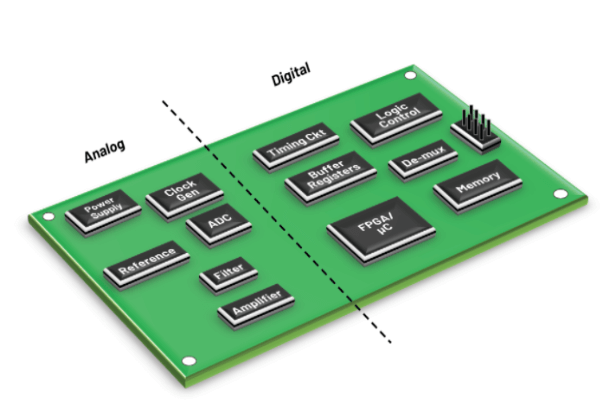
When designing printed circuit boards, the impact of interference on the system should be taken into account. The analog and digital parts of the circuit should be strictly separated. The core circuit should be protected, the system ground wire should be surrounded, and the wiring should be as thick as possible. The power supply should add a filter circuit, DC-DC isolation should be used, and the signal should use photoelectric isolation.
Design an isolated power supply, analyze the parts that are prone to interference (such as clock circuits, communication circuits, etc.) and the parts that are easily interfered (such as analog sampling circuits, etc.), and take measures for these two types of circuits respectively. Take suppression measures for interfering components, take isolation and protection measures for sensitive components, and keep them apart in space and electrical distance.
In board-level design, it is also necessary to pay attention to placing components away from the edge of the printed circuit board, which is beneficial to the protection of air discharge.
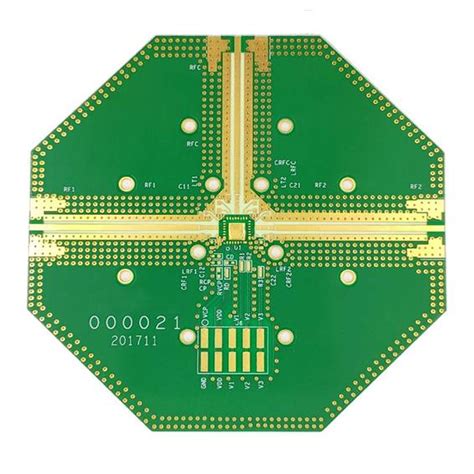
Line spacing: With the continuous improvement and improvement of the manufacturing process of printed circuit boards, it is no longer a problem for general processing plants to produce line spacing equal to or even less than 0.1mm, which can fully meet most applications. Considering the components and production processes used in switching power supplies, the minimum line spacing of double-sided boards is generally set to 0.3mm, and the minimum line spacing of single-sided boards is set to 0.5mm.
The minimum spacing between pads and pads, pads and vias, or vias and vias is set to 0.5mm, which can avoid the “bridging” phenomenon during the welding operation. In this way, most board manufacturers can easily meet production requirements, control the yield rate very high, and achieve a reasonable wiring density and a more economical cost. The minimum line spacing is only suitable for signal control circuits and low-voltage circuits with voltages below 63V. When the line voltage is greater than this value, the line spacing can generally be taken according to the empirical value of 500V/1mm.
Method 1: The circuit board slotting method mentioned above is suitable for some occasions where the spacing is insufficient. By the way, this method is also often used as a protective discharge gap, which is common in the tail plate of the TV picture tube and the AC input of the power supply. This method has been widely used in module power supplies and can achieve good results under potting conditions.
Method 2: Pad insulation paper, which can be made of insulating materials such as green shell paper, polyester film, and polytetrafluoroethylene oriented film. Generally, general power supplies use green shell paper or polyester film to pad between the circuit board and the metal casing. This material has high mechanical strength and has a certain ability to resist moisture. Polytetrafluoroethylene oriented film is widely used in module power supplies due to its high temperature resistance. Insulating film can also be padded between components and surrounding conductors to improve insulation resistance.
The aluminum substrate has the following characteristics due to its own structure: excellent thermal conductivity, single-sided copper bonding, devices can only be placed on the copper bonding surface, and electrical wiring holes cannot be opened, so jumpers cannot be placed like single-sided boards. SMD devices, switch tubes, and output rectifier tubes are generally placed on aluminum substrates to conduct heat away through the substrate.
The thermal resistance is very low and high reliability can be achieved. The transformer adopts a flat SMD structure and can also dissipate heat through the substrate. Its temperature rise is lower than the conventional one. The same specification transformer adopts an aluminum substrate structure to obtain a larger output power. Aluminum substrate jumpers can be handled by bridging.
Aluminum substrate power supplies are generally composed of two printed circuit boards, and the other board is placed on the control circuit. The two boards are physically connected to form a whole. Due to the excellent thermal conductivity of aluminum substrate, it is difficult to manually solder a small amount of soldering. Solder cooling too quickly is prone to problems. There is a simple and practical method. Turn over an ordinary electric iron (preferably with a temperature control function) for ironing clothes, iron the surface upward, fix it, adjust the temperature to about 150℃, put the aluminum substrate on the iron, heat it for a while, and then stick and solder the components according to the conventional method. The iron temperature is suitable for the device to be easy to solder. If it is too high, the device may be damaged or even the copper foil of the aluminum substrate may peel off. If the temperature is too low, the welding effect is not good. It should be mastered flexibly.
Three, some matters about copper foil routing of printed circuit boards
Tracing current density: Most circuits are now made of copper foil bonded to insulating boards. The copper foil thickness of commonly used circuit boards is 35μm. The current density value of the routing can be taken according to the empirical value of 1A/mm. The specific calculation can be referred to the textbook. In principle, the line width should be greater than or equal to 0.3mm to ensure the mechanical strength of the routing.
The copper foil thickness is 70μm. Circuit boards are also commonly used in switching power supplies, so the current density can be higher.
Some products in the module power supply line also use multi-layer boards, which are mainly convenient for integrating power devices such as transformer inductors, optimizing wiring, and heat dissipation of power tubes. It has the advantages of good consistency of process and good heat dissipation of transformers, but its disadvantages are high cost and poor flexibility, and it is only suitable for industrial large-scale production.
Single-sided board, almost all general switching power supplies in the market use single-sided circuit boards, which have the advantage of low cost, and some measures in design and production process can also ensure its performance. In order to ensure good welding mechanical structure performance, the single-sided board pad should be slightly larger to ensure good bonding between the copper foil and the substrate, so as not to peel off or break the copper foil when it is vibrated. Generally, the width of the solder ring should be greater than 0.3mm. The pad hole diameter should be slightly larger than the device pin diameter, but not too large, to ensure that the distance between the pin and the pad is the shortest by solder connection, and the pad hole size should not hinder normal inspection. The pad hole diameter is generally 0.1-0.2mm larger than the pin diameter. Multi-pin devices can also be larger to ensure smooth inspection.
Components on single-sided boards should be close to the circuit board.
For devices that need overhead heat dissipation, sleeves should be added to the pins between the device and the circuit board, which can play a dual role of supporting the device and increasing insulation. It is necessary to minimize or avoid the impact of external force on the connection between the pad and the pin to enhance the firmness of welding. The heavier components on the circuit board can increase the support connection points to strengthen the connection strength between the circuit board, such as transformers and power device heat sinks. The double-sided board pad has a higher strength because the hole has been metallized. The solder ring can be smaller than the single-sided board, and the pad hole diameter can be slightly larger than the pin diameter, because it is conducive to the solder solution to penetrate through the solder hole to the top pad during the welding process to increase welding reliability.
IV. Processing of high current routing
The line width can be processed according to the previous post. If the width is not enough, it can generally be solved by tinning the line to increase the thickness. There are many ways to solve it.
- Set the routing to the pad attribute, so that the routing will not be covered by the solder resist when the circuit board is manufactured, and it will be tinned during hot air leveling.
- Place a pad at the wiring location and set the pad to the shape of the required routing. Be careful to set the pad hole to zero.
- Place the wire on the solder mask layer. This method is the most flexible, but not all circuit board manufacturers will understand your intentions. Textual instructions are required.
The solder mask layer will not be coated with solder mask. Several methods of tinning the circuit are as follows. Generally, a thin strip of tinning can be used with a width of 1~1.5mm, and the length can be determined according to the circuit. The tinned part is spaced 0.5~1mm apart. Double-sided circuit boards provide a lot of options for layout and routing, which can make the routing more reasonable.
Regarding grounding, the power ground and the signal ground must be separated. The two grounds can be combined at the filter capacitor to avoid large pulse currents passing through the signal ground connection and causing unexpected unstable factors. The signal control loop should try to use a single-point grounding method. Voltage feedback sampling, in order to avoid the influence of large currents passing through the wiring, the sampling point of the feedback voltage must be placed at the end of the power output to improve the load effect index of the whole machine. When the wiring changes from one wiring layer to another, vias are generally used for connection. It is not advisable to achieve this through the device pin pads, because this connection relationship may be destroyed when the device is inserted. In addition, there should be at least 2 vias for every 1A current passing through. The via aperture should be greater than 0.5mm in principle. Generally, 0.8mm can ensure processing reliability.


