Precision-Driven Circuit Board Assembly for Durable Electronics

Key Takeaways
Effective PCB assembly relies on precision techniques to ensure electronics withstand demanding operational conditions. Central to this process is advanced soldering, which minimizes thermal stress and prevents joint failures. Automated optical inspection (AOI) systems further enhance accuracy by identifying micro-defects in PCBA workflows.
"Durability in electronics isn’t accidental—it’s engineered through rigorous quality control and material selection." – Industry Expert
For applications in harsh environments (e.g., automotive or aerospace), conformal coating and environmental stress testing are critical. Below is a comparison of key durability-enhancing practices:
| Technique | Purpose | Impact on Longevity |
|---|---|---|
| Automated Soldering | Reduces human error | Improves joint reliability |
| X-Ray Inspection | Detects hidden voids/cracks | Prevents latent failures |
| Thermal Cycling Tests | Simulates extreme temperatures | Validates component resilience |
A tip for manufacturers: Integrate real-time monitoring during PCBA to catch deviations early. Combining statistical process control (SPC) with automated placement systems ensures consistent component alignment, which is vital for high-vibration environments. Transitioning to these methods not only optimizes performance but also aligns with industry standards for durable electronics.
Precision Circuit Board Assembly Techniques
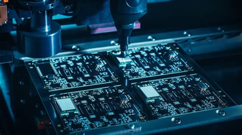
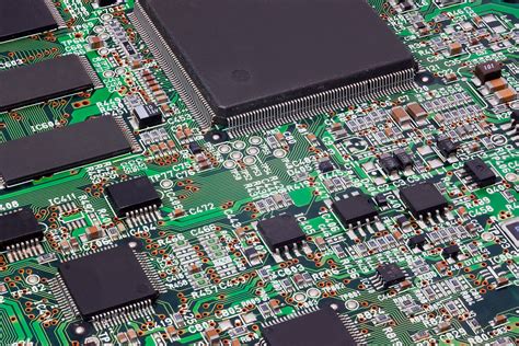
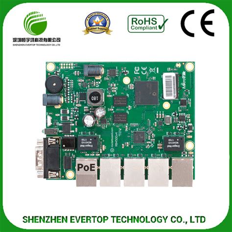
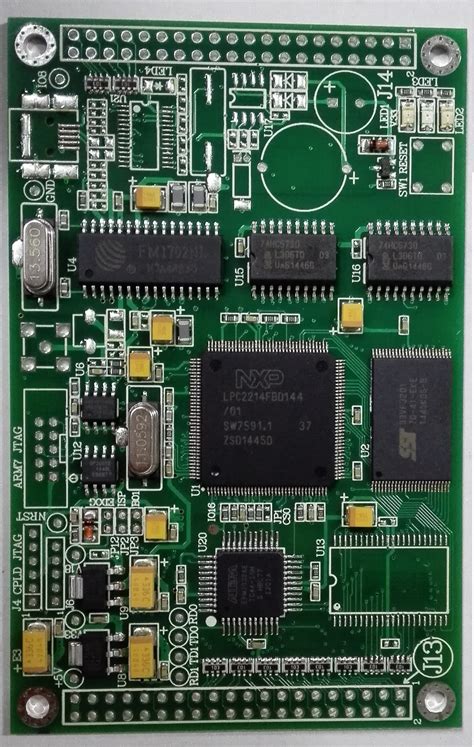
Modern PCB assembly relies on advanced methodologies to achieve the micron-level accuracy required for high-performance electronics. At the core of PCBA (printed circuit board assembly) is the integration of automated systems, such as pick-and-place machines, which position components with tolerances as tight as ±0.01mm. These systems minimize human error while ensuring consistent alignment of surface-mount devices (SMDs) and through-hole components.
Critical to durability is the application of reflow soldering, where precise temperature profiles melt solder paste without damaging sensitive parts. For high-reliability sectors like aerospace, void-free solder joints are non-negotiable, necessitating laser-assisted inspection tools to detect microscopic flaws. Additionally, conformal coating techniques protect assembled boards from moisture, dust, and thermal stress—key for electronics operating in harsh industrial environments.
Transitioning from production to validation, automated optical inspection (AOI) systems cross-verify component placement against design files, flagging deviations that could compromise longevity. This synergy of precision engineering and rigorous testing ensures PCBA outcomes meet MIL-STD-883 standards for shock and vibration resistance. By balancing speed with exactitude, manufacturers deliver circuit boards that power everything from automotive control modules to mission-critical avionics systems.
Optimizing PCB Durability Through Soldering
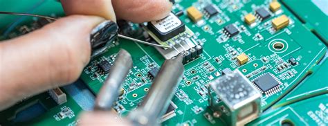
Effective soldering techniques play a central role in enhancing the longevity of PCB assembly (PCBA). Modern electronics manufacturing relies on precision methods like reflow soldering and wave soldering, which ensure consistent joint formation while minimizing thermal stress. For high-reliability applications—such as automotive or aerospace systems—the choice of solder alloy becomes critical. Lead-free SAC305 (tin-silver-copper) alloys, for example, provide robust resistance to thermal cycling and mechanical fatigue, directly influencing the durability of the final product.
Advanced manufacturers employ automated optical inspection (AOI) systems to detect solder defects like voids or cold joints, which compromise structural integrity. Additionally, conformal coatings applied post-soldering shield circuits from moisture, dust, and chemical exposure—common challenges in harsh industrial environments. To balance efficiency and reliability, PCBA processes integrate real-time temperature profiling, ensuring optimal solder flow without damaging heat-sensitive components.
Transitioning to next-gen soldering technologies, such as laser-assisted techniques, further refines precision for microelectronics. These innovations align with stringent quality control protocols, ensuring every solder joint meets IPC-A-610 standards. By prioritizing soldering excellence, manufacturers deliver durable electronics capable of enduring decades of operation, even under extreme conditions.
Automated Component Placement Strategies
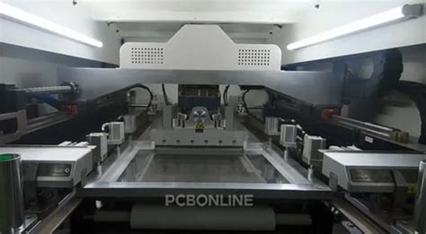
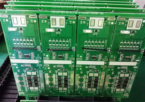
Modern PCB assembly processes rely heavily on automated systems to achieve the micron-level accuracy required for high-performance electronics. Robotic pick-and-place machines, equipped with advanced vision systems, ensure precise alignment of surface-mount devices (SMDs) such as resistors, capacitors, and integrated circuits. These systems analyze component orientation and solder pad geometry in real time, minimizing placement errors that could compromise PCBA reliability. For example, multi-nozzle placement heads enable simultaneous handling of components ranging from 01005-sized passives to large ball grid arrays (BGAs), optimizing throughput without sacrificing precision.
To maintain consistency in high-volume production, manufacturers integrate machine learning algorithms that adapt placement parameters based on component type and board design. This is particularly critical for applications like automotive control modules or aerospace avionics, where vibration resistance and thermal stability are non-negotiable. Additionally, automated optical inspection (AOI) systems work in tandem with placement equipment to flag deviations in real time, creating a closed-loop feedback system.
By streamlining PCB assembly workflows, automation reduces human-induced variability while enabling traceability through digital twin technologies. This foundational accuracy directly supports subsequent stages, such as reflow soldering and functional testing, ensuring seamless alignment with the article’s focus on durable electronics manufacturing.
Quality Control in Electronics Manufacturing
Effective PCB assembly relies on rigorous quality control protocols to ensure the reliability of electronic systems. Modern automated optical inspection (AOI) systems scan PCBA units for soldering defects, misaligned components, or micro-fractures, achieving accuracy rates exceeding 99.9%. For high-density boards, X-ray inspection verifies hidden connections, such as ball grid arrays (BGAs), critical for aerospace and medical devices. Manufacturers also implement In-Circuit Testing (ICT) to validate electrical performance, isolating faults in power distribution or signal integrity before final integration.
To address durability, environmental stress testing simulates extreme temperatures, vibrations, and humidity—key for automotive or industrial applications. Statistical process control (SPC) tools track production metrics, reducing variability in solder paste application or component placement. By combining these methods, PCB assembly workflows minimize failure rates while aligning with ISO 9001 and IPC-A-610 standards. This multi-layered approach not only safeguards product longevity but also reinforces trust in mission-critical electronics.
Reliable PCB Assembly for Harsh Environments
Creating durable electronics for demanding conditions begins with PCB assembly processes designed to withstand extreme temperatures, moisture, vibrations, and chemical exposure. Thermal stress resistance and environmental sealing are prioritized in PCBA workflows, achieved through specialized materials like high-temperature laminates and corrosion-resistant coatings. For industries such as automotive or aerospace, where operational reliability is non-negotiable, manufacturers employ conformal coating techniques to protect circuitry from contaminants, while underfill materials reinforce solder joints against mechanical fatigue.
Automated systems ensure consistent application of protective layers, minimizing human error during component placement and soldering. Rigorous environmental stress screening (ESS) further validates performance under simulated harsh conditions, identifying potential failures before deployment. Advanced PCB assembly protocols also integrate hermetic sealing for critical components, preventing moisture ingress in humid or submerged environments.
To maintain alignment with industry standards like IPC-A-610, quality audits verify compliance with vibration tolerance and thermal cycling requirements. These measures ensure that PCBA outputs meet the longevity demands of industrial machinery, offshore equipment, and military-grade systems. By balancing precision engineering with robust material science, manufacturers deliver electronics capable of thriving in the world’s most unforgiving settings.
Advanced Testing Protocols for Longevity
Robust PCB assembly processes rely on rigorous validation methods to ensure long-term reliability in demanding applications. Advanced testing protocols begin with automated optical inspection (AOI), which detects microscopic defects in solder joints or component alignment with sub-micron precision. For high-density PCBA designs, X-ray inspection complements AOI by examining hidden connections, such as ball grid arrays (BGAs), to prevent latent failures.
Environmental stress testing simulates extreme conditions—thermal cycling (-40°C to +150°C), humidity exposure, and vibration tests—to validate performance under real-world operational stressors. These protocols align with IPC-610 and MIL-STD-883 standards, ensuring boards withstand decades of use in aerospace or automotive systems.
Functional testing further verifies electrical integrity by powering up assemblies and monitoring parameters like current leakage or signal stability. For mission-critical applications, highly accelerated life testing (HALT) pushes components beyond rated limits to identify failure thresholds and refine design margins. By integrating these layered validation steps, manufacturers guarantee that durable electronics meet stringent longevity requirements while minimizing field recalls.
Durable Electronics in Automotive Applications
Modern automotive systems demand PCB assembly solutions capable of withstanding extreme operational conditions, from temperature fluctuations to mechanical vibrations. PCBA processes tailored for vehicles prioritize robust material selection and precision manufacturing to ensure reliability in harsh environments. For instance, high-temperature laminates and conformal coatings protect circuit boards from moisture, dust, and thermal stress, critical for engine control units (ECUs) and advanced driver-assistance systems (ADAS).
Automotive-grade PCB assembly employs automated optical inspection (AOI) to verify component alignment, reducing micro-cracks caused by vibration. Soldering techniques like reflow soldering are optimized for lead-free alloys, enhancing joint durability under repeated thermal cycling. Additionally, vibration-resistant mounting strategies secure connectors and high-mass components, minimizing failure risks in off-road or high-impact scenarios.
Quality control protocols in PCBA for automotive applications include thermal cycling tests and accelerated life testing, simulating decades of use within weeks. These steps validate performance in temperatures ranging from -40°C to 150°C, ensuring compliance with standards like AEC-Q100. By integrating failure mode analysis, manufacturers preemptively address weak points, aligning with automotive safety requirements.
As vehicles evolve toward electrification and autonomy, PCB assembly techniques must balance miniaturization with ruggedness, ensuring longevity without compromising functionality.
Next-Gen Circuit Board Assembly Innovations
The evolution of PCB assembly technologies is reshaping the electronics manufacturing landscape, driven by demands for higher reliability and miniaturization. Innovations such as AI-driven inspection systems and laser-assisted soldering are enhancing precision in PCBA processes, particularly for high-density interconnects (HDIs) and flexible circuits. Advanced pick-and-place robotics, equipped with machine vision, now achieve micron-level accuracy in component positioning, critical for automotive control modules and aerospace avionics.
Emerging materials like nanoparticle-based conductive inks and low-temperature co-fired ceramics (LTCC) are enabling PCB assembly for extreme environments, from sub-zero industrial settings to high-vibration machinery. Simultaneously, IoT-enabled process monitoring provides real-time analytics, optimizing yield rates while reducing thermal stress during reflow soldering. These advancements align with industry shifts toward 3D-printed circuitry and embedded component architectures, which eliminate traditional solder joints to improve longevity.
As sustainability gains priority, innovations in lead-free solder alloys and recyclable substrate materials are being integrated into PCBA workflows, balancing durability with environmental compliance. By combining these technologies, manufacturers can address the growing complexity of smart devices while maintaining the stringent quality standards required for mission-critical applications.
Conclusion
The evolution of PCB assembly (PCBA) methodologies underscores their critical role in developing high-performance electronics for demanding sectors. By prioritizing precision soldering and automated component placement, manufacturers achieve micron-level accuracy, directly enhancing product reliability in automotive, aerospace, and industrial systems. Advanced quality control protocols, such as automated optical inspection (AOI) and X-ray testing, systematically eliminate defects while validating compliance with stringent industry standards.
As industries increasingly operate in extreme environments, PCBA processes now integrate conformal coatings and thermal management solutions to ensure resilience against moisture, vibration, and temperature fluctuations. The adoption of AI-driven analytics further refines PCB assembly workflows, enabling predictive maintenance and real-time process optimization. These innovations not only extend the operational lifespan of electronic devices but also reduce lifecycle costs through preemptive failure detection.
Ultimately, the synergy between robust engineering practices and cutting-edge manufacturing technologies establishes a foundation for next-generation electronics. By maintaining rigorous adherence to durability-focused design principles, the PCBA sector continues to push the boundaries of what modern electronics can achieve in reliability and performance.
Frequently Asked Questions
What distinguishes high-quality PCB assembly from standard processes?
Premium PCBA relies on automated optical inspection and X-ray testing to detect micro-defects. Unlike basic methods, it employs lead-free soldering and thermal profiling to ensure joint integrity under stress.
How does component placement affect electronics durability?
Precision PCB assembly minimizes mechanical strain by aligning components within ±0.05mm tolerances. Automated systems apply force-controlled mounting, reducing cracks in ceramic capacitors or BGA packages during thermal cycling.
Which industries benefit most from ruggedized PCBA?
Automotive and aerospace sectors prioritize conformal coating and underfill encapsulation to combat moisture, vibration, and extreme temperatures. Industrial IoT devices also use vibration-resistant soldering for machinery-mounted electronics.
What testing protocols validate long-term reliability?
Advanced PCB assembly integrates HALT (Highly Accelerated Life Testing) and IST (Interconnect Stress Testing). These simulate decades of operational wear in days, identifying weak points in trace routing or via structures.
Can PCBA techniques reduce environmental failure risks?
Yes. Ionic contamination testing and humidity resistance grading ensure boards withstand corrosive atmospheres. Selective soldering also prevents flux residues from degrading high-frequency circuits.
Ready to Elevate Your Electronics’ Lifespan?
For tailored PCB assembly solutions meeting MIL-STD-883 standards, please click here to consult our engineering team.