Precision-Driven Double Layer PCB Manufacturing Expertise
Key Takeaways
When engaging with PCB manufacturing partners, understanding core engineering principles becomes crucial for project success. You’ll want to prioritize suppliers that combine precision layer alignment with advanced etching techniques—both critical for minimizing signal loss in double-layer PCB designs. Leading PCB manufacturing companies leverage ISO-certified processes to ensure traceability, from material selection to final testing, reducing defects by up to 30% compared to non-certified providers^1^.
| Cost Factor | Impact on PCB Manufacturing Cost | Optimization Strategy |
|---|---|---|
| Material Selection | 40-50% of total cost | Use industry-grade FR-4 substrates |
| Prototyping Speed | Reduces time-to-market by 35% | Partner with rapid-turn services |
| Quality Assurance | Lowers failure rates by 22% | Implement automated AOI systems |
Balancing PCB manufacturing business objectives with technical requirements requires aligning design complexity with production scalability. For instance, opting for standardized panel sizes can trim PCB manufacturing cost by 15–20% without compromising performance. Meanwhile, rigorous testing protocols—like thermal cycling and impedance checks—ensure reliability across industrial, automotive, or IoT applications. By focusing on these pillars, you secure cost-effective, high-yield solutions that align with evolving electronics demands.
[^1^]: Learn how ISO certification enhances PCB quality
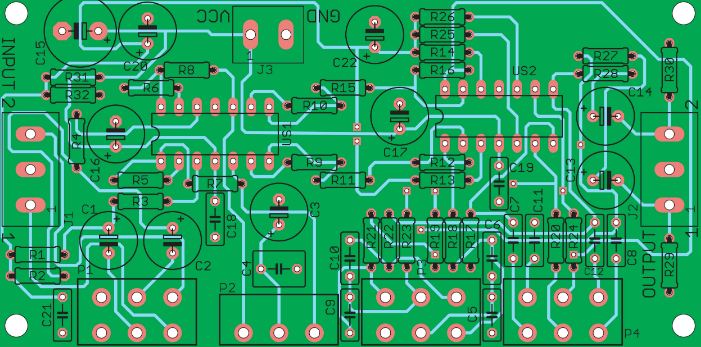
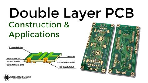
Precision 2-Layer PCB Engineering Essentials
Achieving precision in PCB manufacturing begins with meticulous design and material selection. When engineering double-layer boards, you must balance electrical performance with manufacturability—optimal trace widths, spacing, and via placement ensure signal integrity while minimizing PCB manufacturing cost. FR-4 substrates remain the industry standard, but specialized materials like high-Tg laminates may be required for thermally demanding applications.
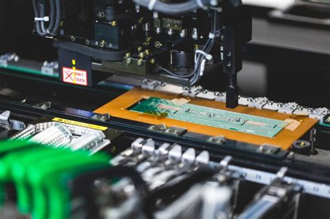
Leading PCB manufacturing companies employ advanced laser drilling and automated optical inspection (AOI) systems to maintain ±0.075mm tolerance levels, critical for high-density interconnects. A well-optimized design not only reduces material waste but also accelerates production timelines, a key advantage for startups managing tight PCB manufacturing business budgets.
"Always validate your Gerber files with DFM (Design for Manufacturing) checks—this preemptive step can prevent costly reworks and delays during prototyping."
When evaluating PCB manufacturing cost, consider factors like solder mask options, copper weight, and surface finishes (e.g., ENIG vs. HASL). By collaborating with certified partners early in the design phase, you can align technical specifications with cost-effective production strategies without compromising reliability.
Rigorous Quality Control in PCB Fabrication
When selecting PCB manufacturing companies for your double-layer boards, understanding their quality assurance protocols is critical. Modern PCB manufacturing relies on multi-stage inspection systems, beginning with automated optical inspection (AOI) to detect micro-defects in copper traces and solder masks. Advanced thermal testing further validates material integrity under operational stress, ensuring your design withstands real-world conditions.
Cost-conscious projects benefit from stringent quality controls, as they reduce post-production failures that inflate PCB manufacturing cost. Reputable providers implement cross-sectional analysis and electrical testing to verify layer alignment and impedance matching—key factors for high-frequency applications. By prioritizing traceability and documentation, these processes align with ISO standards, creating a foundation for scalable PCB manufacturing business operations.
Transitioning from prototyping to mass production becomes seamless when manufacturers integrate statistical process control (SPC) tools. These systems monitor critical parameters like etch rates and lamination pressures, maintaining consistency across batches. For innovators balancing performance and budget, robust quality frameworks ensure reliability without compromising affordability—a hallmark of strategic partnerships in electronics development.
ISO-Certified Double Layer PCB Processes
When selecting PCB manufacturing companies for your double-layer boards, ISO-certified processes ensure adherence to globally recognized quality benchmarks. These standards govern every stage—from material selection to final inspection—guaranteeing consistency in traceability, process validation, and corrective action protocols. Certified facilities employ advanced imaging systems and automated testing to detect micro-defects, minimizing risks of signal interference or thermal stress in high-frequency applications.
By prioritizing ISO-compliant PCB manufacturing, you benefit from streamlined workflows that reduce material waste and rework, directly impacting PCB manufacturing cost efficiency. For instance, controlled solder mask application and precision drilling under certified conditions prevent costly errors like misalignment or copper over-etching. This translates to faster turnaround times without compromising the dimensional accuracy required for complex circuitry.
For businesses scaling their PCB manufacturing business, certification serves as a market differentiator. Clients in aerospace, automotive, or medical sectors often mandate ISO compliance to meet regulatory obligations. Partnering with certified manufacturers not only ensures product reliability but also future-proofs your supply chain against evolving industry standards. Rigorous documentation practices further simplify audits, accelerating time-to-market for mission-critical electronics.
Rapid Prototyping for Electronics Innovation
When developing cutting-edge electronics, rapid prototyping transforms conceptual designs into functional PCB manufacturing proofs within days. Leading PCB manufacturing companies leverage advanced laser drilling and automated optical inspection (AOI) to accelerate iterative testing while maintaining precision. This approach lets you validate circuit layouts, component placements, and thermal management strategies before committing to full-scale production—a critical step for avoiding costly redesigns.
By integrating PCB manufacturing cost optimization into prototyping workflows, engineers balance material selection and layer complexity without compromising performance. For instance, using cost-effective FR-4 substrates with optimized copper weights reduces waste while meeting signal integrity requirements. The ability to test multiple iterations quickly ensures design flaws are resolved early, directly lowering long-term production risks.
For businesses scaling their PCB manufacturing business, rapid prototyping supports faster time-to-market for IoT devices, wearables, and industrial controllers. Whether you’re refining high-frequency circuits or compact consumer electronics, this methodology bridges innovation and commercialization—ensuring your final product aligns with both technical specifications and market demands. The agility of modern prototyping systems also enables seamless transitions from 2-layer prototypes to complex multilayer configurations as project requirements evolve.
Cost-Effective Solutions for 2-Layer PCBs
When optimizing PCB manufacturing expenses for 2-layer designs, balancing performance and affordability requires strategic planning. Leading PCB manufacturing companies leverage standardized material inventories and automated workflows to reduce PCB manufacturing cost while maintaining quality. By prioritizing design simplicity—such as minimizing via counts and avoiding unnecessary trace complexity—you can lower material waste and production time. For prototypes or mid-volume runs, opting for panelized designs maximizes substrate utilization, further cutting per-unit expenses.
To ensure cost efficiency, evaluate suppliers offering transparent pricing models that align with your PCB manufacturing business needs. Many providers now offer tiered pricing for bulk orders, enabling scalability without compromising turnaround times. Advanced design-for-manufacturing (DFM) tools also play a critical role, identifying potential flaws early to avoid costly revisions. While lower-cost options exist, verify that suppliers adhere to industry standards (e.g., IPC Class 2) to prevent reliability issues that could inflate long-term expenses.
Finally, consider hybrid approaches: combining rapid prototyping for iterative testing with volume production for finalized designs. This strategy minimizes upfront investment while maintaining flexibility for design adjustments, ensuring your 2-layer PCBs meet both technical and budgetary requirements.
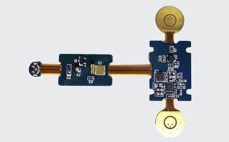
Advanced Double Layer PCB Applications
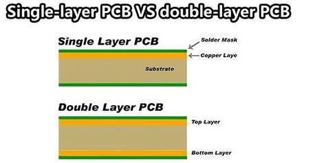
When designing electronics that demand both functionality and compactness, PCB manufacturing solutions for double-layer boards become indispensable. These PCBs serve as the backbone for applications where space optimization and signal integrity are critical—think wearable devices, automotive control modules, or industrial sensors. By leveraging the dual conductive layers, PCB manufacturing companies can route complex circuits while maintaining a slim profile, ideal for modern consumer electronics or IoT ecosystems.
In automotive systems, for instance, double-layer boards handle engine management units and infotainment systems, balancing PCB manufacturing cost with robust performance. Their adaptability also shines in renewable energy technologies, such as solar inverters, where thermal management and durability are non-negotiable. For prototyping or mid-volume production, partnering with a PCB manufacturing business that offers design-for-manufacturability (DFM) feedback ensures your layouts align with fabrication realities, minimizing revisions.
Transitioning from single to double-layer designs often unlocks cost efficiencies without sacrificing reliability—a strategic move when scaling production. Whether you’re developing medical wearables or smart home devices, understanding how layer stacking and material selection influence signal interference and power distribution ensures your application thrives in competitive markets. This flexibility makes double-layer PCBs a cornerstone for innovation across industries.
Optimized Manufacturing for High-Performance PCBs
When developing PCB manufacturing strategies for high-performance applications, precision and adaptability define success. Modern double-layer PCBs demand meticulous attention to material selection, trace geometry, and thermal management to meet stringent electrical requirements. Leading PCB manufacturing companies leverage automated optical inspection (AOI) and impedance-controlled routing to minimize signal loss, ensuring boards perform reliably under high-frequency or high-power conditions.
Balancing PCB manufacturing cost with performance starts with design-for-manufacturability (DFM) principles. By optimizing layer stack-ups and reducing via complexity, you can achieve faster production cycles without compromising quality—a critical advantage in competitive industries like automotive or IoT. Additionally, advanced surface finishes such as ENIG or immersion silver enhance durability while maintaining cost efficiency.
For businesses scaling their PCB manufacturing business, investing in flexible prototyping systems allows rapid iteration of high-performance designs. This approach not only accelerates time-to-market but also reduces waste through data-driven process adjustments. Whether you’re refining existing products or exploring cutting-edge applications, optimized workflows ensure your double-layer PCBs deliver both technical excellence and economic viability.
Ensuring Reliability in Multilayer PCB Production
When scaling from double-layer PCB manufacturing to multilayer designs, reliability becomes paramount due to increased complexity. Advanced alignment systems and material selection protocols form the backbone of consistent performance, particularly when PCB manufacturing companies handle intricate layer stacking. You’ll find that rigorous testing—such as automated optical inspection (AOI) and thermal cycling—ensures interlayer connections withstand operational stresses, reducing failure risks in high-density applications.
Balancing PCB manufacturing cost with quality requires optimizing layer count, material grades, and via structures. For instance, using high-Tg laminates or controlled impedance materials might elevate initial expenses but extend product lifespans in demanding environments. Signal integrity analysis and cross-sectional inspections further validate design choices, aligning with ISO-certified processes mentioned earlier.
In the PCB manufacturing business, partnerships with certified suppliers for prepregs and copper foils enhance traceability. This becomes critical when addressing thermal management in multilayer boards, where uneven heat distribution can compromise reliability. By integrating design-for-manufacturability (DFM) feedback early, you mitigate rework costs and accelerate time-to-market—key considerations when transitioning from prototyping to full-scale production.
Conclusion
When selecting PCB manufacturing partners for your double-layer designs, prioritize PCB manufacturing companies that demonstrate mastery in precision engineering and scalable solutions. The right partner balances PCB manufacturing cost efficiency with uncompromising quality—critical for maintaining competitiveness in the electronics sector. By leveraging ISO-certified processes, you ensure traceability and consistency, whether prototyping or scaling production.
For businesses managing tight timelines, rapid prototyping capabilities minimize lead times while validating design integrity early. This approach not only accelerates innovation but also reduces risks in your PCB manufacturing business by catching flaws before full-scale production.
Ultimately, optimizing double-layer PCB manufacturing hinges on aligning technical expertise with your project’s unique demands. From thermal management to signal integrity, every layer must meet high-performance standards to ensure end-product reliability. By understanding cost drivers—material selection, testing protocols, and volume thresholds—you can make informed decisions that enhance both technical outcomes and financial viability.
FAQs
What distinguishes quality-focused PCB manufacturing for 2-layer boards?
Reputable PCB manufacturing companies prioritize material selection, controlled impedance, and automated optical inspection (AOI) to ensure signal integrity. Their processes align with ISO 9001 standards, minimizing defects in high-frequency or power-sensitive designs.
How does PCB manufacturing cost vary for double-layer prototypes?
Costs depend on board complexity, material grades, and lead times. While simpler designs might cost $0.05 per square inch, advanced requirements like ENIG surface finishes or tight tolerances increase pricing. Many providers offer tiered pricing for bulk orders.
Why partner with specialized PCB manufacturing business providers?
Expert manufacturers optimize stack-up configurations and thermal management for your application, whether IoT devices or industrial controls. They reduce risks like delamination or solder bridging, critical for long-term reliability in harsh environments.
Can rapid prototyping reduce time-to-market for 2-layer PCBs?
Yes. Advanced facilities combine laser direct imaging and automated routing to deliver prototypes in 24–48 hours. This agility lets you test EMI performance or mechanical fit early, accelerating product iterations.
Ready to Optimize Your Double Layer PCB Project?
For precision-driven PCB manufacturing solutions tailored to your technical requirements, please click here to consult with industry experts. Streamline your production timeline while maintaining rigorous quality benchmarks.